DSP1
Superclocked Member

- Total Posts : 216
- Reward points : 0
- Joined: 2016/09/19 14:49:55
- Status: offline
- Ribbons : 1


Re: bad(HOT) PCB Layout on GTX 1070 FTW?
2016/10/31 07:25:22
(permalink)
whitezero
brokencross
whitezero
brokencross
whitezero
I think they're basically saying that regardless of if you do the thermal pad mod or not, EVGA's 3 year warranty applies in this case. So if your VRM explodes 3.1 years down the road, you're probably not going to be able to get a free replacement.
Yeah, that's exactly what worries me. Either way, I'll probably install the thermal pads just for peace of mind.
For sure, seems like an . And in the process, you can opt to put on a higher quality TIM (thermal paste) for the GPU itself for even better thermals than before the mod. I've been considering going with the GELID GC-Extreme, myself.
Yeah. I still have a bit of AS5, but I'll probably get a good ceramic based paste.
Yeah AS5 may not be the best choice, there are a lot of other paste's out there that do a better job on GPUs. http://www.tomshardware.c...benchmark,3616-20.html
And EVGA may include some paste with the mod as well.
Tom's Hardware??? Are you sure that the testing they do there is reliable? 

|
Leonardohlb
Superclocked Member
- Total Posts : 177
- Reward points : 0
- Joined: 2012/01/18 06:14:29
- Location: Bonfim-MG, Brazil
- Status: offline
- Ribbons : 1
Re: bad(HOT) PCB Layout on GTX 1070 FTW?
2016/10/31 07:26:48
(permalink)
dzernesto
11.0W/mk ?!?!?!? JEZZZZZ
Where I'll find those, the best I found is a Arctic with 6.0 W/mK
EDIT: well, googling for 11.0W/mk, there is plenty out there. But it is expensive...
You live in Brazil like me? Just found 16.0w / mK in ML, this is for GPU not mosfet, but i think it can be similar.
|
dzernesto
New Member

- Total Posts : 40
- Reward points : 0
- Joined: 2013/09/23 13:41:10
- Location: Brazil
- Status: offline
- Ribbons : 0
Re: bad(HOT) PCB Layout on GTX 1070 FTW?
2016/10/31 07:29:31
(permalink)
Leonardohlb
dzernesto
11.0W/mk ?!?!?!? JEZZZZZ
Where I'll find those, the best I found is a Arctic with 6.0 W/mK
EDIT: well, googling for 11.0W/mk, there is plenty out there. But it is expensive...
You live in Brazil like me? Just found 16.0w / mK in ML, this is for GPU not mosfet, but i think it can be similar.
Yes Brazilian here! Can you share the link you found?
|
DSP1
Superclocked Member
- Total Posts : 216
- Reward points : 0
- Joined: 2016/09/19 14:49:55
- Status: offline
- Ribbons : 1
Re: bad(HOT) PCB Layout on GTX 1070 FTW?
2016/10/31 07:30:34
(permalink)
Leonardohlb
whitezero
Leonardohlb
EVGA should release a video showing where to install the pad thermal so that customers could do without waiting for sending the thermal pads.
Well you'll also need the right size/shape thermal pad as well, to make proper contact and not effect the mounting pressure on the other components. I think overall it's best to wait for EVGA's own provided pads.
When i wanted to change the thermal pad i contacted the evga by ticket they told me it can be any thermal pad 1.0mm thick, and at least 11.0 W / mK.
"I apologize for the inconvenience but unfortunately we don't sell those or have any to give out since they already come pre-installed from the factory. However, you can purchase those online and the thickness is 1.0mm.
We are here 24/7 if you have other questions or concerns, thank you."
Saudções,
EVGA
image
"We don't have any brand that we can recommend but you can use 11.0 W/mK for conductivity."
Saudções,
EVGA
image
This is very interesting because when I contacted Tech Support about the types of pads they use they told me they use Shin Etsu. So I went to the Shin Etsu website and looked at the types of pads that they have available and none of them are rated 11.0w/mK. http://www.shinetsusilico.../heat_rubb/index.shtml
|
dzernesto
New Member
- Total Posts : 40
- Reward points : 0
- Joined: 2013/09/23 13:41:10
- Location: Brazil
- Status: offline
- Ribbons : 0
Re: bad(HOT) PCB Layout on GTX 1070 FTW?
2016/10/31 07:32:46
(permalink)
|
DSP1
Superclocked Member
- Total Posts : 216
- Reward points : 0
- Joined: 2016/09/19 14:49:55
- Status: offline
- Ribbons : 1
Re: bad(HOT) PCB Layout on GTX 1070 FTW?
2016/10/31 07:36:16
(permalink)
dzernesto
deleted
I didn't see that. Best I saw was 4.0 or something. Did I miss a page? Got a link please?
|
evgauser28764
Superclocked Member
- Total Posts : 232
- Reward points : 0
- Joined: 2016/07/01 06:27:49
- Status: offline
- Ribbons : 0
Re: bad(HOT) PCB Layout on GTX 1070 FTW?
2016/10/31 07:37:31
(permalink)
Leonardohlb
acxcoolerssuck
Leonardohlb
whitezero
Leonardohlb
EVGA should release a video showing where to install the pad thermal so that customers could do without waiting for sending the thermal pads.
Well you'll also need the right size/shape thermal pad as well, to make proper contact and not effect the mounting pressure on the other components. I think overall it's best to wait for EVGA's own provided pads.
When i wanted to change the thermal pad i contacted the evga by ticket they told me it can be any thermal pad 1.0mm thick, and at least 11.0 W / mK.
"I apologize for the inconvenience but unfortunately we don't sell those or have any to give out since they already come pre-installed from the factory. However, you can purchase those online and the thickness is 1.0mm.
We are here 24/7 if you have other questions or concerns, thank you."
Saudções,
EVGA
image
"We don't have any brand that we can recommend but you can use 11.0 W/mK for conductivity."
Saudções,
EVGA
image
thermal pad is soft, so dont buy 1mm, go for 1.5mm will be better, imo
Excuse me this thermal pad is not for the mosfet but for the GPU, probably for that mosfet is 2.0mm
i am saying vram pad evga using is 1mm, vrm pad is 2mm. if you want to replace them , you better try 0.5mm more for perfect contact. i already tried to add thermal pads to the back of the pcb when i first got the card and was using the stock cooler. those impression are still there even a month later. but this may bend your backplate a little. 
|
dzernesto
New Member
- Total Posts : 40
- Reward points : 0
- Joined: 2013/09/23 13:41:10
- Location: Brazil
- Status: offline
- Ribbons : 0
Re: bad(HOT) PCB Layout on GTX 1070 FTW?
2016/10/31 07:38:09
(permalink)
DSP1
dzernesto
deleted
I didn't see that. Best I saw was 4.0 or something.
Did I miss a page? Got a link please?
My information was wrong, I was looking into fluid compounds.
post edited by dzernesto - 2016/10/31 07:46:48
|
DSP1
Superclocked Member
- Total Posts : 216
- Reward points : 0
- Joined: 2016/09/19 14:49:55
- Status: offline
- Ribbons : 1
Re: bad(HOT) PCB Layout on GTX 1070 FTW?
2016/10/31 07:46:16
(permalink)
acxcoolerssuck
Leonardohlb
acxcoolerssuck
Leonardohlb
whitezero
Leonardohlb
EVGA should release a video showing where to install the pad thermal so that customers could do without waiting for sending the thermal pads.
Well you'll also need the right size/shape thermal pad as well, to make proper contact and not effect the mounting pressure on the other components. I think overall it's best to wait for EVGA's own provided pads.
When i wanted to change the thermal pad i contacted the evga by ticket they told me it can be any thermal pad 1.0mm thick, and at least 11.0 W / mK.
"I apologize for the inconvenience but unfortunately we don't sell those or have any to give out since they already come pre-installed from the factory. However, you can purchase those online and the thickness is 1.0mm.
We are here 24/7 if you have other questions or concerns, thank you."
Saudções,
EVGA
image
"We don't have any brand that we can recommend but you can use 11.0 W/mK for conductivity."
Saudções,
EVGA
image
thermal pad is soft, so dont buy 1mm, go for 1.5mm will be better, imo
Excuse me this thermal pad is not for the mosfet but for the GPU, probably for that mosfet is 2.0mm
i am saying vram pad evga using is 1mm, vrm pad is 2mm.
if you want to replace them , you better try 0.5mm more for perfect contact.
i already tried to add thermal pads to the back of the pcb when i first got the card and was using the stock cooler. those impression are still there even a month later.
but this may bend your backplate a little.
So those are all pads you applied yourself? And they are all the same thickness?
|
evgauser28764
Superclocked Member
- Total Posts : 232
- Reward points : 0
- Joined: 2016/07/01 06:27:49
- Status: offline
- Ribbons : 0
Re: bad(HOT) PCB Layout on GTX 1070 FTW?
2016/10/31 08:02:32
(permalink)
DSP1
acxcoolerssuck
Leonardohlb
acxcoolerssuck
Leonardohlb
whitezero
Leonardohlb
EVGA should release a video showing where to install the pad thermal so that customers could do without waiting for sending the thermal pads.
Well you'll also need the right size/shape thermal pad as well, to make proper contact and not effect the mounting pressure on the other components. I think overall it's best to wait for EVGA's own provided pads.
When i wanted to change the thermal pad i contacted the evga by ticket they told me it can be any thermal pad 1.0mm thick, and at least 11.0 W / mK.
"I apologize for the inconvenience but unfortunately we don't sell those or have any to give out since they already come pre-installed from the factory. However, you can purchase those online and the thickness is 1.0mm.
We are here 24/7 if you have other questions or concerns, thank you."
Saudções,
EVGA
image
"We don't have any brand that we can recommend but you can use 11.0 W/mK for conductivity."
Saudções,
EVGA
image
thermal pad is soft, so dont buy 1mm, go for 1.5mm will be better, imo
Excuse me this thermal pad is not for the mosfet but for the GPU, probably for that mosfet is 2.0mm
i am saying vram pad evga using is 1mm, vrm pad is 2mm.
if you want to replace them , you better try 0.5mm more for perfect contact.
i already tried to add thermal pads to the back of the pcb when i first got the card and was using the stock cooler. those impression are still there even a month later.
but this may bend your backplate a little.
So those are all pads you applied yourself?
And they are all the same thickness?
sure, when i got the card in august. these are 2.5mm, but the plate will be slightly bent. these are 3m 8810. the gap between pcb and back plate is 2mm. so i chose 2.5mm. worked great, the plate was very hot during gaming, cant put my figure on the plate for few seconds. i remove the back plate when i change to aio cooling. these pads cant be removed after used... and two sides of the pad are different, if you wrongly place them, the these pad will be on the pcb 
|
Leonardohlb
Superclocked Member
- Total Posts : 177
- Reward points : 0
- Joined: 2012/01/18 06:14:29
- Location: Bonfim-MG, Brazil
- Status: offline
- Ribbons : 1
Re: bad(HOT) PCB Layout on GTX 1070 FTW?
2016/10/31 08:08:47
(permalink)
DSP1
Leonardohlb
whitezero
Leonardohlb
EVGA should release a video showing where to install the pad thermal so that customers could do without waiting for sending the thermal pads.
Well you'll also need the right size/shape thermal pad as well, to make proper contact and not effect the mounting pressure on the other components. I think overall it's best to wait for EVGA's own provided pads.
When i wanted to change the thermal pad i contacted the evga by ticket they told me it can be any thermal pad 1.0mm thick, and at least 11.0 W / mK.
"I apologize for the inconvenience but unfortunately we don't sell those or have any to give out since they already come pre-installed from the factory. However, you can purchase those online and the thickness is 1.0mm.
We are here 24/7 if you have other questions or concerns, thank you."
Saudções,
EVGA
image
"We don't have any brand that we can recommend but you can use 11.0 W/mK for conductivity."
Saudções,
EVGA
image
This is very interesting because when I contacted Tech Support about the types of pads they use they told me they use Shin Etsu.
So I went to the Shin Etsu website and looked at the types of pads that they have available and none of them are rated 11.0w/mK.
http://www.shinetsusilico.../heat_rubb/index.shtml

|
whitezero
New Member
- Total Posts : 50
- Reward points : 0
- Joined: 2008/01/31 22:04:35
- Status: offline
- Ribbons : 0
Re: bad(HOT) PCB Layout on GTX 1070 FTW?
2016/10/31 08:11:48
(permalink)
DSP1
whitezero
brokencross
whitezero
brokencross
whitezero
I think they're basically saying that regardless of if you do the thermal pad mod or not, EVGA's 3 year warranty applies in this case. So if your VRM explodes 3.1 years down the road, you're probably not going to be able to get a free replacement.
Yeah, that's exactly what worries me. Either way, I'll probably install the thermal pads just for peace of mind.
For sure, seems like an . And in the process, you can opt to put on a higher quality TIM (thermal paste) for the GPU itself for even better thermals than before the mod. I've been considering going with the GELID GC-Extreme, myself.
Yeah. I still have a bit of AS5, but I'll probably get a good ceramic based paste.
Yeah AS5 may not be the best choice, there are a lot of other paste's out there that do a better job on GPUs. http://www.tomshardware.c...benchmark,3616-20.html
And EVGA may include some paste with the mod as well.
Tom's Hardware???
Are you sure that the testing they do there is reliable?
Not a lot of sites do large scale TIM testing like this. Did you have some specific beef with TomsHardware? Can't say I'm aware of glaring inaccuracies with their testing over the years.
12G-P5-3967-KR 6/3/2021 7:46:49 AM PT NO
AMD Ryzen 7 5800X |==| Noctua NH-U12AMSI X570 Unify |==| EVGA RTX 3070 XC3 Ultra32GB G.SKILL Ripjaws V 3600 CL16 (Samsung B-Die) |==| Adata XPG 8200 Pro 2TB Windows 10 Pro |==| Fractal Define 7 Compact |==| Corsair RM850x PSU
|
Leonardohlb
Superclocked Member
- Total Posts : 177
- Reward points : 0
- Joined: 2012/01/18 06:14:29
- Location: Bonfim-MG, Brazil
- Status: offline
- Ribbons : 1
Re: bad(HOT) PCB Layout on GTX 1070 FTW?
2016/10/31 08:18:36
(permalink)
This was the most effective solution i found to cool the back, an AMD processor 6cm cooler connected with pins reversed 5~7 volts, enough to cool and not generate noise. 
|
Leonardohlb
Superclocked Member
- Total Posts : 177
- Reward points : 0
- Joined: 2012/01/18 06:14:29
- Location: Bonfim-MG, Brazil
- Status: offline
- Ribbons : 1
Re: bad(HOT) PCB Layout on GTX 1070 FTW?
2016/10/31 08:20:12
(permalink)
dzernesto
Leonardohlb
dzernesto
11.0W/mk ?!?!?!? JEZZZZZ
Where I'll find those, the best I found is a Arctic with 6.0 W/mK
EDIT: well, googling for 11.0W/mk, there is plenty out there. But it is expensive...
You live in Brazil like me? Just found 16.0w / mK in ML, this is for GPU not mosfet, but i think it can be similar.
Yes Brazilian here!
Can you share the link you found?
Check your private message.
|
NucleusX
Superclocked Member
- Total Posts : 240
- Reward points : 0
- Joined: 2014/09/15 22:58:17
- Status: offline
- Ribbons : 0
Re: bad(HOT) PCB Layout on GTX 1070 FTW?
2016/10/31 08:23:18
(permalink)
acxcoolerssuck
sure, when i got the card in august. these are 2.5mm, but the plate will be slightly bent.
these are 3m 8810.
the gap between pcb and back plate is 2mm. so i chose 2.5mm.
worked great, the plate was very hot during gaming, cant put my figure on the plate for few seconds.
i remove the back plate when i change to aio cooling.
these pads cant be removed after used...
and two sides of the pad are different, if you wrongly place them, the these pad will be on the pcb
I'm surprised i didn't even think to check this while it was in my machine. Observing a warmer back-plate might actually be a good thing. Could mean its doing a better job at extracting more heat away from those components. After having done all your thermals, do you feel its improved your situation all-round ?
CPU: Intel 486 DX2. 66Mhz (Turbo). Cooling: LN2.
MTB: ECS. Chipset: SIS. HD: WD Raptor 300mb x 512. 154GB. Raid 0.
RAM: Corsair Obliterator Gold. EDO. 16mb. 66mhz. x8.
GPU: Nvidia GTX Riva TNT2 FTW OC. PCI. 32mb. x4 Quad SLI.
PSU: ATX 200 watt (no label). Case: RGB Milk Crate.
|
brokencross
New Member
- Total Posts : 89
- Reward points : 0
- Joined: 2016/10/04 06:36:07
- Status: offline
- Ribbons : 0
Re: bad(HOT) PCB Layout on GTX 1070 FTW?
2016/10/31 08:25:34
(permalink)
Leonardohlb
This was the most effective solution i found to cool the back, an AMD processor 6cm cooler connected with pins reversed 5~7 volts, enough to cool and not generate noise.
That's pretty ingenious. My fan setup allows for direct air flow towards the card so it never really gets too top-hot. 
Intel i5 4690K@4.4Ghz | MSI Z97 Gaming 5 | EVGA GTX1070 FTW replaced by a MSI GTX 1070 Gaming X | G.Skill RipJawsX 8GB 1866Mhz | Corsair CS650M | Thermalright Macho | NZXT S340
|
NucleusX
Superclocked Member
- Total Posts : 240
- Reward points : 0
- Joined: 2014/09/15 22:58:17
- Status: offline
- Ribbons : 0
Re: bad(HOT) PCB Layout on GTX 1070 FTW?
2016/10/31 08:28:27
(permalink)
I believe the back-plate can both be beneficial and problematic simultaneously. Some components will suffer more with it on, and
others will suffer less without it. A side panel fan blowing at the cards edge might be a good idea if the back-plate is a concern.
CPU: Intel 486 DX2. 66Mhz (Turbo). Cooling: LN2.
MTB: ECS. Chipset: SIS. HD: WD Raptor 300mb x 512. 154GB. Raid 0.
RAM: Corsair Obliterator Gold. EDO. 16mb. 66mhz. x8.
GPU: Nvidia GTX Riva TNT2 FTW OC. PCI. 32mb. x4 Quad SLI.
PSU: ATX 200 watt (no label). Case: RGB Milk Crate.
|
Leonardohlb
Superclocked Member
- Total Posts : 177
- Reward points : 0
- Joined: 2012/01/18 06:14:29
- Location: Bonfim-MG, Brazil
- Status: offline
- Ribbons : 1
Re: bad(HOT) PCB Layout on GTX 1070 FTW?
2016/10/31 08:35:49
(permalink)
brokencross
Leonardohlb
This was the most effective solution i found to cool the back, an AMD processor 6cm cooler connected with pins reversed 5~7 volts, enough to cool and not generate noise.
That's pretty ingenious.
My fan setup allows for direct air flow towards the card so it never really gets too top-hot.
I did not use the CPU cooler, here it is pulling hot air up, but this cooler 6cm even with low speed cooling very well backplate, you have room to use a 9cm or 12cm slim, do not even modify the position of the noctua.
|
NucleusX
Superclocked Member
- Total Posts : 240
- Reward points : 0
- Joined: 2014/09/15 22:58:17
- Status: offline
- Ribbons : 0
Re: bad(HOT) PCB Layout on GTX 1070 FTW?
2016/10/31 08:37:45
(permalink)
One thing that hasn't been mentioned or covered much in testing is how the fans pull in reverse on the ACX 3.0 instead of push.
CPU: Intel 486 DX2. 66Mhz (Turbo). Cooling: LN2.
MTB: ECS. Chipset: SIS. HD: WD Raptor 300mb x 512. 154GB. Raid 0.
RAM: Corsair Obliterator Gold. EDO. 16mb. 66mhz. x8.
GPU: Nvidia GTX Riva TNT2 FTW OC. PCI. 32mb. x4 Quad SLI.
PSU: ATX 200 watt (no label). Case: RGB Milk Crate.
|
Leonardohlb
Superclocked Member
- Total Posts : 177
- Reward points : 0
- Joined: 2012/01/18 06:14:29
- Location: Bonfim-MG, Brazil
- Status: offline
- Ribbons : 1
Re: bad(HOT) PCB Layout on GTX 1070 FTW?
2016/10/31 08:38:53
(permalink)
NucleusX
I believe the back-plate can both be beneficial and problematic simultaneously. Some components will suffer more with it on, and
others will suffer less without it. A side panel fan blowing at the cards edge might be a good idea if the back-plate is a concern.
Dust and not as effective as a cooler on top, i tested.
|
Leonardohlb
Superclocked Member
- Total Posts : 177
- Reward points : 0
- Joined: 2012/01/18 06:14:29
- Location: Bonfim-MG, Brazil
- Status: offline
- Ribbons : 1
Re: bad(HOT) PCB Layout on GTX 1070 FTW?
2016/10/31 08:41:33
(permalink)
NucleusX
One thing that hasn't been mentioned or covered much in testing is how the fans pull in reverse on the ACX 3.0 instead of push.
Depending on the direction of the airflow in the case, can be a good solution.
|
NucleusX
Superclocked Member
- Total Posts : 240
- Reward points : 0
- Joined: 2014/09/15 22:58:17
- Status: offline
- Ribbons : 0
Re: bad(HOT) PCB Layout on GTX 1070 FTW?
2016/10/31 08:50:28
(permalink)
Leonardohlb
NucleusX
I believe the back-plate can both be beneficial and problematic simultaneously. Some components will suffer more with it on, and
others will suffer less without it. A side panel fan blowing at the cards edge might be a good idea if the back-plate is a concern.
Dust and not as effective as a cooler on top, i tested.
Not surprising. Leonardohlb
NucleusX
One thing that hasn't been mentioned or covered much in testing is how the fans pull in reverse on the ACX 3.0 instead of push.
Depending on the direction of the airflow in the case, can be a good solution.
Could also be problemtic with the wrong airflow. People would need to take that into account with correctly oriented case fans.
CPU: Intel 486 DX2. 66Mhz (Turbo). Cooling: LN2.
MTB: ECS. Chipset: SIS. HD: WD Raptor 300mb x 512. 154GB. Raid 0.
RAM: Corsair Obliterator Gold. EDO. 16mb. 66mhz. x8.
GPU: Nvidia GTX Riva TNT2 FTW OC. PCI. 32mb. x4 Quad SLI.
PSU: ATX 200 watt (no label). Case: RGB Milk Crate.
|
evgauser28764
Superclocked Member
- Total Posts : 232
- Reward points : 0
- Joined: 2016/07/01 06:27:49
- Status: offline
- Ribbons : 0
Re: bad(HOT) PCB Layout on GTX 1070 FTW?
2016/10/31 08:55:44
(permalink)
NucleusX
acxcoolerssuck
sure, when i got the card in august. these are 2.5mm, but the plate will be slightly bent.
these are 3m 8810.
the gap between pcb and back plate is 2mm. so i chose 2.5mm.
worked great, the plate was very hot during gaming, cant put my figure on the plate for few seconds.
i remove the back plate when i change to aio cooling.
these pads cant be removed after used...
and two sides of the pad are different, if you wrongly place them, the these pad will be on the pcb
I'm surprised i didn't even think to check this while it was in my machine. Observing a warmer back-plate
might actually be a good thing. Could mean its doing a better job at extracting more heat away from those
components. After having done all your thermals, do you feel its improved your situation all-round ?
sure, hotter back plate means heat of the back of the pcb are spreading to the plate. no i dont feel any differences as the stock cooling is too weak, 75c~80c during gaming at~2025mhz.
|
Leonardohlb
Superclocked Member
- Total Posts : 177
- Reward points : 0
- Joined: 2012/01/18 06:14:29
- Location: Bonfim-MG, Brazil
- Status: offline
- Ribbons : 1
Re: bad(HOT) PCB Layout on GTX 1070 FTW?
2016/10/31 09:00:09
(permalink)
acxcoolerssuck
NucleusX
acxcoolerssuck
sure, when i got the card in august. these are 2.5mm, but the plate will be slightly bent.
these are 3m 8810.
the gap between pcb and back plate is 2mm. so i chose 2.5mm.
worked great, the plate was very hot during gaming, cant put my figure on the plate for few seconds.
i remove the back plate when i change to aio cooling.
these pads cant be removed after used...
and two sides of the pad are different, if you wrongly place them, the these pad will be on the pcb
I'm surprised i didn't even think to check this while it was in my machine. Observing a warmer back-plate
might actually be a good thing. Could mean its doing a better job at extracting more heat away from those
components. After having done all your thermals, do you feel its improved your situation all-round ?
sure, hotter back plate means heat of the back of the pcb are spreading to the plate.
no i dont feel any differences as the stock cooling is too weak, 75c~80c during gaming at~2025mhz.
Use a cooler as i used, i want to see if it will make no difference...  use also mode agressive in EVGA precision.
|
NucleusX
Superclocked Member
- Total Posts : 240
- Reward points : 0
- Joined: 2014/09/15 22:58:17
- Status: offline
- Ribbons : 0
Re: bad(HOT) PCB Layout on GTX 1070 FTW?
2016/10/31 09:02:26
(permalink)
acxcoolerssuck
sure, hotter back plate means heat of the back of the pcb are spreading to the plate.
no i dont feel any differences as the stock cooling is too weak, 75c~80c during gaming at~2025mhz.
Well there's also pads making contact with the back of the GPU, so now when your VRMs go up, some of that heat will shift back to your GPU and vice versa now that they are linked by the same cooling surface. By that point, your kinda fighting a losing battle for achieving any reasonable temp reductions i'd say. Diminishing returns.
post edited by NucleusX - 2016/10/31 09:05:56
CPU: Intel 486 DX2. 66Mhz (Turbo). Cooling: LN2.
MTB: ECS. Chipset: SIS. HD: WD Raptor 300mb x 512. 154GB. Raid 0.
RAM: Corsair Obliterator Gold. EDO. 16mb. 66mhz. x8.
GPU: Nvidia GTX Riva TNT2 FTW OC. PCI. 32mb. x4 Quad SLI.
PSU: ATX 200 watt (no label). Case: RGB Milk Crate.
|
evgauser28764
Superclocked Member
- Total Posts : 232
- Reward points : 0
- Joined: 2016/07/01 06:27:49
- Status: offline
- Ribbons : 0
Re: bad(HOT) PCB Layout on GTX 1070 FTW?
2016/10/31 09:06:23
(permalink)
NucleusX
acxcoolerssuck
sure, hotter back plate means heat of the back of the pcb are spreading to the plate.
no i dont feel any differences as the stock cooling is too weak, 75c~80c during gaming at~2025mhz.
Well there's also pads making contact with the back of the GPU, so now when your VRMs go up, some of that heat will shift back to your GPU and vice versa
now that they are linked by the same cooling surface. By that point, your kinda fighting a losing battle for achieving any reasonable temp reductions i'd say.
that pads near gpu are the stock pads, i think these are for preventing the backplate to hurt the pcb but not spreading heat. you are right, but that is the limitation though. using cooling plate, not just evga but other brands like msi and galax, helps reducing gpu temp as the heat from vrm and gpu are separated. if evga acx3.0 has no cooling plate but actively cooled the vrm by the main heatsink, then in my case my ftw may reach 80c~85c. so the nature of the problem is the acx heatsink is not good and powerful enough for some high ambient temp situation and bad airflow cases. i mean, asia is where evga does not well take care of. it is no doubt that under ~20C ambient temp, with acx 3.0 the gpu temp will be around 67c. but in south asia 20c is very rare.
post edited by acxcoolerssuck - 2016/10/31 09:12:45
|
NucleusX
Superclocked Member
- Total Posts : 240
- Reward points : 0
- Joined: 2014/09/15 22:58:17
- Status: offline
- Ribbons : 0
Re: bad(HOT) PCB Layout on GTX 1070 FTW?
2016/10/31 09:12:30
(permalink)
acxcoolerssuck
that pads near gpu are the stock pads, i think these are for preventing the backplate to hurt the pcb but not spreading heat.
Not so sure about that tbh, the GPU pads material seemed to be very similar to the memory thermal pads. The stock ones at-least.
CPU: Intel 486 DX2. 66Mhz (Turbo). Cooling: LN2.
MTB: ECS. Chipset: SIS. HD: WD Raptor 300mb x 512. 154GB. Raid 0.
RAM: Corsair Obliterator Gold. EDO. 16mb. 66mhz. x8.
GPU: Nvidia GTX Riva TNT2 FTW OC. PCI. 32mb. x4 Quad SLI.
PSU: ATX 200 watt (no label). Case: RGB Milk Crate.
|
evgauser28764
Superclocked Member
- Total Posts : 232
- Reward points : 0
- Joined: 2016/07/01 06:27:49
- Status: offline
- Ribbons : 0
Re: bad(HOT) PCB Layout on GTX 1070 FTW?
2016/10/31 09:15:17
(permalink)
NucleusX
acxcoolerssuck
that pads near gpu are the stock pads, i think these are for preventing the backplate to hurt the pcb but not spreading heat.
Not so sure about that tbh, the GPU pads material seemed to be very similar to the memory thermal pads. The stock ones at-least.
if that little pads are for cooling, then i think evga should have used the same gpu pad in arctic hybrid 140. 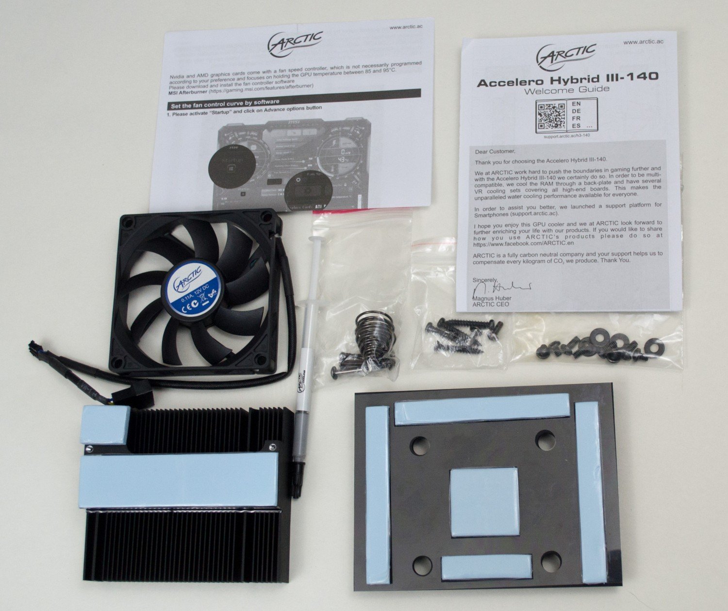
|
bcavnaugh
The Crunchinator

- Total Posts : 38516
- Reward points : 0
- Joined: 2012/09/18 17:31:18
- Location: USA Affiliate E5L3CTGE12 Associate 9E88QK5L7811G3H
- Status: offline
- Ribbons : 282
Re: bad(HOT) PCB Layout on GTX 1070 FTW?
2016/10/31 09:15:18
(permalink)
It all so looks like this will block air flow between your PCB and Back Plate. I would re-review what you are doing here and also use the correct size of them pads as you do not want to bend the Back Plate. This may lead to bending the PCB and even cracking the PCB.
post edited by bcavnaugh - 2016/10/31 09:18:25
|
DSP1
Superclocked Member
- Total Posts : 216
- Reward points : 0
- Joined: 2016/09/19 14:49:55
- Status: offline
- Ribbons : 1
Re: bad(HOT) PCB Layout on GTX 1070 FTW?
2016/10/31 09:37:05
(permalink)
whitezero
DSP1
whitezero
brokencross
whitezero
brokencross
whitezero
I think they're basically saying that regardless of if you do the thermal pad mod or not, EVGA's 3 year warranty applies in this case. So if your VRM explodes 3.1 years down the road, you're probably not going to be able to get a free replacement.
Yeah, that's exactly what worries me. Either way, I'll probably install the thermal pads just for peace of mind.
For sure, seems like an . And in the process, you can opt to put on a higher quality TIM (thermal paste) for the GPU itself for even better thermals than before the mod. I've been considering going with the GELID GC-Extreme, myself.
Yeah. I still have a bit of AS5, but I'll probably get a good ceramic based paste.
Yeah AS5 may not be the best choice, there are a lot of other paste's out there that do a better job on GPUs. http://www.tomshardware.c...benchmark,3616-20.html
And EVGA may include some paste with the mod as well.
Tom's Hardware???
Are you sure that the testing they do there is reliable?
Not a lot of sites do large scale TIM testing like this. Did you have some specific beef with TomsHardware? Can't say I'm aware of glaring inaccuracies with their testing over the years.
Was a joke. The whole issue started from a review by Toms Hardware.DE that EVGA says is not reliable.
|