Emwun Garand
New Member

- Total Posts : 47
- Reward points : 0
- Joined: 2016/10/19 11:26:25
- Status: offline
- Ribbons : 0

Re: bad(HOT) PCB Layout on GTX 1070 FTW?
2016/10/20 12:14:39
(permalink)
It might be worth the time for EVGA to basically chop the heat spreading backing plate in half between the VRM and VRAM. That way the heat doesn't transfer so easily across the metal from one to the other. The only other alternative seems to be to run a very aggressive fan profile and just cope with having a GE90115b in your office.
|
NetQvist
New Member
- Total Posts : 56
- Reward points : 0
- Joined: 2016/09/01 08:18:01
- Status: offline
- Ribbons : 0
Re: bad(HOT) PCB Layout on GTX 1070 FTW?
2016/10/20 12:32:38
(permalink)
Emwun Garand
It might be worth the time for EVGA to basically chop the heat spreading backing plate in half between the VRM and VRAM. That way the heat doesn't transfer so easily across the metal from one to the other. The only other alternative seems to be to run a very aggressive fan profile and just cope with having a GE90115b in your office.
Maybe that's what they meant by not releasing the information about the issue so that people won't try to fix it themselves and void their warranty! Haha! =)
|
NeroRay
New Member
- Total Posts : 19
- Reward points : 0
- Joined: 2016/10/17 08:11:26
- Status: offline
- Ribbons : 0
Re: bad(HOT) PCB Layout on GTX 1070 FTW?
2016/10/20 12:53:26
(permalink)
I really hope we are going to get a response from evga soon
|
AHowes
CLASSIFIED ULTRA Member

- Total Posts : 6502
- Reward points : 0
- Joined: 2005/09/20 15:38:10
- Location: Macomb MI
- Status: offline
- Ribbons : 27
Re: bad(HOT) PCB Layout on GTX 1070 FTW?
2016/10/20 13:02:17
(permalink)
Emwun Garand
It might be worth the time for EVGA to basically chop the heat spreading backing plate in half between the VRM and VRAM. That way the heat doesn't transfer so easily across the metal from one to the other. The only other alternative seems to be to run a very aggressive fan profile and just cope with having a GE90115b in your office.
Why not try it and see?
Intel i9 9900K @ 5.2Ghz Single HUGE Custom Water Loop. Asus Z390 ROG Extreme XI MB G.Skill Trident Z 32GB (4x8GB) 4266MHz DDR4 EVGA 2080ti K|NGP|N w/ Hydro Copper block. 34" Dell Alienware AW3418DW 1440 Ultra Wide GSync Monitor Thermaltake Core P7 Modded w/ 2x EK Dual D5 pump top,2 x EK XE 480 2X 360 rads.1 Corsair 520 Rad.
|
Emwun Garand
New Member
- Total Posts : 47
- Reward points : 0
- Joined: 2016/10/19 11:26:25
- Status: offline
- Ribbons : 0
Re: bad(HOT) PCB Layout on GTX 1070 FTW?
2016/10/20 15:25:44
(permalink)
AHowes
Emwun Garand
It might be worth the time for EVGA to basically chop the heat spreading backing plate in half between the VRM and VRAM. That way the heat doesn't transfer so easily across the metal from one to the other. The only other alternative seems to be to run a very aggressive fan profile and just cope with having a GE90115b in your office.
Why not try it and see?
I'd be happy to do the fabrication and testing if they want to provide me with a free FTW.
|
Triss
New Member
- Total Posts : 79
- Reward points : 0
- Joined: 2013/11/04 21:17:45
- Status: offline
- Ribbons : 0
Re: bad(HOT) PCB Layout on GTX 1070 FTW?
2016/10/20 23:05:08
(permalink)
Interesting times ahead i guess for us FTW owners
|
zfkjswf
New Member
- Total Posts : 5
- Reward points : 0
- Joined: 2016/09/18 13:08:43
- Status: offline
- Ribbons : 0
Re: bad(HOT) PCB Layout on GTX 1070 FTW?
2016/10/21 03:42:13
(permalink)
are all 1070 ftw cards affected by this issue? are all cards shipped before 31 aug automatically eligible for rma?
|
mannitu78
New Member
- Total Posts : 33
- Reward points : 0
- Joined: 2015/12/18 07:15:18
- Status: offline
- Ribbons : 0
Re: bad(HOT) PCB Layout on GTX 1070 FTW?
2016/10/21 04:09:33
(permalink)
there are 2 Issues atm. 1 about the micron memory, which you can fix with a bios update (as far as i know)..and this one, of course it does affect all cards. It doesnt have to affect all users. It depends what type of games you play, if you overclock, benchmark etc. I guess it may only become a problem with high power draw. However, i think the RMA-sendback-rate will be outstanding high with this FTW series. Its not the gpu-temp that kills cards over time, but the temperature of the pcb and the soldering, the very high temp-differences put a lot of stress on the vram and the solderings all around the gpu-socket. But with EVGA at least you should not get a problem when you have to return it.
post edited by mannitu78 - 2016/10/21 04:13:53
|
the_Scarlet_one
formerly Scarlet-tech

- Total Posts : 24080
- Reward points : 0
- Joined: 2013/11/13 02:48:57
- Location: East Coast
- Status: offline
- Ribbons : 79

Re: bad(HOT) PCB Layout on GTX 1070 FTW?
2016/10/21 04:11:28
(permalink)
zfkjswf
are all 1070 ftw cards affected by this issue? are all cards shipped before 31 aug automatically eligible for rma?
Not every card is affected by the same issues, but if your card is having an issue, then an RMA is warranted. There more than likely isn't a set timeline as to which cards see issues compared to others, since every card isn't affected the same.
|
mannitu78
New Member
- Total Posts : 33
- Reward points : 0
- Joined: 2015/12/18 07:15:18
- Status: offline
- Ribbons : 0
Re: bad(HOT) PCB Layout on GTX 1070 FTW?
2016/10/21 04:50:59
(permalink)
Guys, seriously, you should consider to buy a Raijintek Morpheus or an EK Alpenfön Peter...see this as an oppurtunity..every PCB that costs a couple of 100 bucks deserves high-end-air cooling. Theres just no way a stock cooler will ever be able to keep up. Theres just no enough room under stock coolers to provide really good heatsinks on VRM and memory. And 2x120mm ist just superior to 2x100 or 3x90mm..... 
|
EVGA_JacobF
EVGA Alumni

- Total Posts : 11559
- Reward points : 0
- Joined: 2006/01/17 12:10:20
- Location: Brea, CA
- Status: offline
- Ribbons : 26
Re: bad(HOT) PCB Layout on GTX 1070 FTW?
2016/10/21 12:27:54
(permalink)
Please see below message:
“The test used in the referenced review from Toms Hardware (Germany) is running under Furmark, an extreme usage case, as most overclockers know. We believe this is a good approach to have some idea about the graphics card limit, and the thermal performance under the worst case scenario. EVGA has performed a similar qualification test during the design process, at a higher ambient temperature (30C in chamber) with a thermal coupler probe directly contacting the key components and after the Toms Hardware (Germany) review, we have retested this again. The results in both tests show the temperature of PWM and memory is within the spec tolerance under the same stress test, and is working as originally designed with no issues.
With this being said, EVGA understands that lower temperatures are preferred by reviewers and customers.
During our recent testing, we have applied additional thermal pads between the backplate and the PCB and between the baseplate and the heatsink fins, with the results shown below. We will offer these optional thermal pads free of charge to EVGA owners who want to have a lower temperature. These thermal pads will be ready soon; and customers can request them on Monday, October 24th, 2016. Also, we will work with Toms Hardware to do a retest.”
Thanks,
EVGA
EVGA GeForce GTX 1080 FTW running Furmark with thermal pad mod (30C Ambient in Chamber) – October 21st, 2016
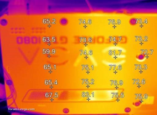
Attached Image(s)

|
the_Scarlet_one
formerly Scarlet-tech
- Total Posts : 24080
- Reward points : 0
- Joined: 2013/11/13 02:48:57
- Location: East Coast
- Status: offline
- Ribbons : 79
Re: bad(HOT) PCB Layout on GTX 1070 FTW?
2016/10/21 12:33:49
(permalink)
EVGA_JacobF
Please see below message:
“The test used in the referenced review from Toms Hardware (Germany) is running under Furmark, an extreme usage case, as most overclockers know. We believe this is a good approach to have some idea about the graphics card limit, and the thermal performance under the worst case scenario. EVGA has performed a similar qualification test during the design process, at a higher ambient temperature (30C in chamber) with a thermal coupler probe directly contacting the key components and after the Toms Hardware (Germany) review, we have retested this again. The results in both tests show the temperature of PWM and memory is within the spec tolerance under the same stress test, and is working as originally designed with no issues.
With this being said, EVGA understands that lower temperatures are preferred by reviewers and customers.
During our recent testing, we have applied additional thermal pads between the backplate and the PCB and between the baseplate and the heatsink fins, with the results shown below. We will offer these optional thermal pads free of charge to EVGA owners who want to have a lower temperature. These thermal pads will be ready soon; and customers can request them on Monday, October 24th, 2016. Also, we will work with Toms Hardware to do a retest.”
Thanks,
EVGA
EVGA GeForce GTX 1080 FTW running Furmark with thermal pad mod (30C Ambient in Chamber) – October 21st, 2016
Jacob, thank you all for looking into this.
|
AHowes
CLASSIFIED ULTRA Member
- Total Posts : 6502
- Reward points : 0
- Joined: 2005/09/20 15:38:10
- Location: Macomb MI
- Status: offline
- Ribbons : 27
Re: bad(HOT) PCB Layout on GTX 1070 FTW?
2016/10/21 12:39:53
(permalink)
Now that's evga for ya! Can't see any other video card company paying attention to there customers!
Intel i9 9900K @ 5.2Ghz Single HUGE Custom Water Loop. Asus Z390 ROG Extreme XI MB G.Skill Trident Z 32GB (4x8GB) 4266MHz DDR4 EVGA 2080ti K|NGP|N w/ Hydro Copper block. 34" Dell Alienware AW3418DW 1440 Ultra Wide GSync Monitor Thermaltake Core P7 Modded w/ 2x EK Dual D5 pump top,2 x EK XE 480 2X 360 rads.1 Corsair 520 Rad.
|
relevance
New Member
- Total Posts : 91
- Reward points : 0
- Joined: 2009/04/01 17:26:20
- Status: offline
- Ribbons : 0
Re: bad(HOT) PCB Layout on GTX 1070 FTW?
2016/10/21 12:41:06
(permalink)
will these thermal pads be compatible with Hydro Copper owners? I'm ready to buy the block once it's available to purchase. just waiting..
|
the_Scarlet_one
formerly Scarlet-tech
- Total Posts : 24080
- Reward points : 0
- Joined: 2013/11/13 02:48:57
- Location: East Coast
- Status: offline
- Ribbons : 79
Re: bad(HOT) PCB Layout on GTX 1070 FTW?
2016/10/21 12:42:39
(permalink)
relevance
will these thermal pads be compatible with Hydro Copper owners? I'm ready to buy the block once it's available to purchase. just waiting..
The hydrocopper should not need anything like this, as water will be actively cooling the VRM section through the block.
|
howdy2u2
FTW Member

- Total Posts : 1896
- Reward points : 0
- Joined: 2006/12/01 04:31:48
- Status: offline
- Ribbons : 6
Re: bad(HOT) PCB Layout on GTX 1070 FTW?
2016/10/21 12:51:06
(permalink)
Scarlet-Tech
relevance
will these thermal pads be compatible with Hydro Copper owners? I'm ready to buy the block once it's available to purchase. just waiting..
The hydrocopper should not need anything like this, as water will be actively cooling the VRM section through the block.
Also if you look at the photos on the product page, the block already has them installed. Peel the clear tape off and install....I'm sure the instructions will inform you of this. Taken from the Overview page on the product page: "and the full-cover block cools GPU, Memory and VRM. EVGA has already pre-installed thermal pads to remove the inconvenience of having to guess and cut the pads yourself to make it a hassle-free installation.
post edited by howdy2u2 - 2016/10/21 12:55:49
|
the_Scarlet_one
formerly Scarlet-tech
- Total Posts : 24080
- Reward points : 0
- Joined: 2013/11/13 02:48:57
- Location: East Coast
- Status: offline
- Ribbons : 79
Re: bad(HOT) PCB Layout on GTX 1070 FTW?
2016/10/21 12:55:00
(permalink)
howdy2u2
Scarlet-Tech
relevance
will these thermal pads be compatible with Hydro Copper owners? I'm ready to buy the block once it's available to purchase. just waiting..
The hydrocopper should not need anything like this, as water will be actively cooling the VRM section through the block.
Also if you look at the photos on the product page, the block already has them installed. Peel the clear tape off and install....I'm sure the instructions will inform you of this.
The thermal pad you are referring to is on the block. The thermal pad the other user is inquiring about is in between the pcb and backplate. *edit* The one "between the base plate and heatsink fins" would not be applicable because of the base plate being removed to install a waterblock.
post edited by Scarlet-Tech - 2016/10/21 13:00:29
|
howdy2u2
FTW Member
- Total Posts : 1896
- Reward points : 0
- Joined: 2006/12/01 04:31:48
- Status: offline
- Ribbons : 6
Re: bad(HOT) PCB Layout on GTX 1070 FTW?
2016/10/21 12:56:11
(permalink)
Scarlet-Tech
howdy2u2
Scarlet-Tech
relevance
will these thermal pads be compatible with Hydro Copper owners? I'm ready to buy the block once it's available to purchase. just waiting..
The hydrocopper should not need anything like this, as water will be actively cooling the VRM section through the block.
Also if you look at the photos on the product page, the block already has them installed. Peel the clear tape off and install....I'm sure the instructions will inform you of this.
The thermal pad you are referring to is on the block. The thermal pad the other user is inquiring about is in between the pcb and backplate.
Okkkkkkkk, Ill hush now ........... 
|
Emwun Garand
New Member
- Total Posts : 47
- Reward points : 0
- Joined: 2016/10/19 11:26:25
- Status: offline
- Ribbons : 0
Re: bad(HOT) PCB Layout on GTX 1070 FTW?
2016/10/21 13:15:17
(permalink)
BAM! That's what I call customer service. I will be requesting my pads on Monday and am 100% happy that I chose EVGA! Thank you guys for responding so quickly and coming up with a solution to give customers peace of mind.
|
bairanbokkeri
New Member
- Total Posts : 18
- Reward points : 0
- Joined: 2016/09/17 13:41:45
- Status: offline
- Ribbons : 0
Re: bad(HOT) PCB Layout on GTX 1070 FTW?
2016/10/21 13:19:44
(permalink)
I was already contemplating on going with a full custom water setup, so those pads might actually save me some 600 euros or so. :D
|
SirMoh
New Member
- Total Posts : 20
- Reward points : 0
- Joined: 2016/09/21 06:09:08
- Status: offline
- Ribbons : 0
Re: bad(HOT) PCB Layout on GTX 1070 FTW?
2016/10/21 13:26:30
(permalink)
EVGA_JacobF
Please see below message:
“The test used in the referenced review from Toms Hardware (Germany) is running under Furmark, an extreme usage case, as most overclockers know. We believe this is a good approach to have some idea about the graphics card limit, and the thermal performance under the worst case scenario. EVGA has performed a similar qualification test during the design process, at a higher ambient temperature (30C in chamber) with a thermal coupler probe directly contacting the key components and after the Toms Hardware (Germany) review, we have retested this again. The results in both tests show the temperature of PWM and memory is within the spec tolerance under the same stress test, and is working as originally designed with no issues.
With this being said, EVGA understands that lower temperatures are preferred by reviewers and customers.
During our recent testing, we have applied additional thermal pads between the backplate and the PCB and between the baseplate and the heatsink fins, with the results shown below. We will offer these optional thermal pads free of charge to EVGA owners who want to have a lower temperature. These thermal pads will be ready soon; and customers can request them on Monday, October 24th, 2016. Also, we will work with Toms Hardware to do a retest.”
Thanks,
EVGA
EVGA GeForce GTX 1080 FTW running Furmark with thermal pad mod (30C Ambient in Chamber) – October 21st, 2016
Does this also apply to the 1070 FTW?
|
libneon
New Member
- Total Posts : 90
- Reward points : 0
- Joined: 2005/09/08 15:20:38
- Status: offline
- Ribbons : 0
Re: bad(HOT) PCB Layout on GTX 1070 FTW?
2016/10/21 13:31:46
(permalink)
EVGA_JacobF
Please see below message:
“The test used in the referenced review from Toms Hardware (Germany) is running under Furmark, an extreme usage case, as most overclockers know. We believe this is a good approach to have some idea about the graphics card limit, and the thermal performance under the worst case scenario. EVGA has performed a similar qualification test during the design process, at a higher ambient temperature (30C in chamber) with a thermal coupler probe directly contacting the key components and after the Toms Hardware (Germany) review, we have retested this again. The results in both tests show the temperature of PWM and memory is within the spec tolerance under the same stress test, and is working as originally designed with no issues.
With this being said, EVGA understands that lower temperatures are preferred by reviewers and customers.
During our recent testing, we have applied additional thermal pads between the backplate and the PCB and between the baseplate and the heatsink fins, with the results shown below. We will offer these optional thermal pads free of charge to EVGA owners who want to have a lower temperature. These thermal pads will be ready soon; and customers can request them on Monday, October 24th, 2016. Also, we will work with Toms Hardware to do a retest.”
Thanks,
EVGA
EVGA GeForce GTX 1080 FTW running Furmark with thermal pad mod (30C Ambient in Chamber) – October 21st, 2016

Thanks so much for the update. My 1070 FTW was shipped back for an RMA because it caught fire right along the hot VRM area- will my replacement card have these thermal pads installed?
|
relevance
New Member
- Total Posts : 91
- Reward points : 0
- Joined: 2009/04/01 17:26:20
- Status: offline
- Ribbons : 0
Re: bad(HOT) PCB Layout on GTX 1070 FTW?
2016/10/21 13:32:07
(permalink)
Scarlet-Tech
relevance
will these thermal pads be compatible with Hydro Copper owners? I'm ready to buy the block once it's available to purchase. just waiting..
The hydrocopper should not need anything like this, as water will be actively cooling the VRM section through the block.
good to know. didn't know if there was some gap between the block and the hotspot. I thought thermal pads might seal the gap. my FTW is only thing that's not in loop, can't wait.
|
melao
New Member
- Total Posts : 3
- Reward points : 0
- Joined: 2014/02/04 09:13:43
- Status: offline
- Ribbons : 0
Re: bad(HOT) PCB Layout on GTX 1070 FTW?
2016/10/21 13:43:11
(permalink)
Since this looks like the only place EVGA is answering, I bought a 1080 FTW DT while ago, I live in a hot country (35C ambient), EVGA will ship the thermal pad for me free of shipping charge? Also, to install the thermal pad you need to open the graphics card, dont it loose the warranty? Its funny because lots of people are having problems the card blowing up, blackscreen, and according to you guys, the temp in 30C test is OK, so why this kind of problem is happening? Everyone who buys a 1070/1080 have a proper case and fans.
|
the_Scarlet_one
formerly Scarlet-tech
- Total Posts : 24080
- Reward points : 0
- Joined: 2013/11/13 02:48:57
- Location: East Coast
- Status: offline
- Ribbons : 79
Re: bad(HOT) PCB Layout on GTX 1070 FTW?
2016/10/21 13:48:41
(permalink)
relevance
Scarlet-Tech
relevance
will these thermal pads be compatible with Hydro Copper owners? I'm ready to buy the block once it's available to purchase. just waiting..
The hydrocopper should not need anything like this, as water will be actively cooling the VRM section through the block.
good to know. didn't know if there was some gap between the block and the hotspot. I thought thermal pads might seal the gap. my FTW is only thing that's not in loop, can't wait.
There is a thermal pad that goes between the pcb and the block for sure. Waterblocks do very well at cooling vrm.
|
Brenex
New Member
- Total Posts : 7
- Reward points : 0
- Joined: 2016/09/05 08:47:51
- Status: offline
- Ribbons : 0
Re: bad(HOT) PCB Layout on GTX 1070 FTW?
2016/10/21 14:12:30
(permalink)
libneon
Thanks so much for the update. My 1070 FTW was shipped back for an RMA because it caught fire right along the hot VRM area- will my replacement card have these thermal pads installed?
I second this question. I just shipped my 1070 FTW in yesterday so it should arrive at the RMA facility next week. Will my RMA replacement for coil whine have the new pads installed already or should I request them?
|
steve1873
New Member
- Total Posts : 17
- Reward points : 0
- Joined: 2016/07/28 17:55:19
- Status: offline
- Ribbons : 1
Re: bad(HOT) PCB Layout on GTX 1070 FTW?
2016/10/21 15:48:40
(permalink)
I have a SC 1080, however have since replaced it with GTX Hybrid kit. How is that cooler set for cooling of that section of VRM's?
I certainly don't wish to take it apart again to inspect, so could someone from EVGA please comment.
|
EllBrad
New Member
- Total Posts : 69
- Reward points : 0
- Joined: 2016/06/15 12:51:39
- Location: Canada
- Status: offline
- Ribbons : 0
Re: bad(HOT) PCB Layout on GTX 1070 FTW?
2016/10/21 16:03:40
(permalink)
A. Are these for the FTW models only or normal PCB models as well, (SC edition)
B. There will obviously be a shipping fee, so can they be shipped in combination with the powerlink(s) when that program goes live on November 1st?
i5 4690k @ 4.5ghz | EVGA GTX 1070SC @ 2.1ghz | 16gb DDR3 @ 1866mhz | Acer XB270HU
|
the_Scarlet_one
formerly Scarlet-tech
- Total Posts : 24080
- Reward points : 0
- Joined: 2013/11/13 02:48:57
- Location: East Coast
- Status: offline
- Ribbons : 79
Re: bad(HOT) PCB Layout on GTX 1070 FTW?
2016/10/21 16:09:38
(permalink)
steve1873
I have a SC 1080, however have since replaced it with GTX Hybrid kit. How is that cooler set for cooling of that section of VRM's?
I certainly don't wish to take it apart again to inspect, so could someone from EVGA please comment.
The hybrid utilizes a base plate for the VRM just like the Founders Edition has.
|
bitxan
New Member
- Total Posts : 67
- Reward points : 0
- Joined: 2014/03/31 13:50:22
- Status: offline
- Ribbons : 0
Re: bad(HOT) PCB Layout on GTX 1070 FTW?
2016/10/21 16:10:21
(permalink)
I understand that the charge for the Powerlink gift .... but the cost of the pads ,,,, please be serious EVGA ...
|