xWinti
New Member

- Total Posts : 8
- Reward points : 0
- Joined: 2021/05/08 03:50:39
- Status: offline
- Ribbons : 0

Hey, so I'm a guy that buys dead or broken gaming peripherals usually mechanical keyboards, mice, headsets, and then I repair them. I recently received this GTX 970 FTW that had 2 burnt out mosfets and although the card is alive, the mosfets prevent the pc from booting. Since, I don't have much experience with fixing gpu, I needed some help and here's what's going on. One mosfet is stuck to its pad and the pad isn't connected to the PCB itself (Ill include a picture). So I have a couple questions, the mosfet code is 4C10N RCD 6 Ohms found at Q15 and Q22 (both of them have the same code). I couldn't find any mosfet with the same name online I did find 4C10N mosfets but they always had a different codes after it, like, 4C10N RAM8B or 4C10N NT1G. Do these mosfets work as a replacement? or do I need a replacement with the same name as the burnt ones? Next is the pad connecting the mosfet to the PCB, do I need a new one? or does the old one work fine? and If I need a new one How's the procedure to installing it? Lastly is the PCB itself (area under the pad), Do I need to do anything regarding it? Please, if you could help me that would be really appreciated and I know a lot of people might say to pass it on since I'm a beginner. But I got this gpu solely for the sake of learning and fixing it. Thanks a lot! 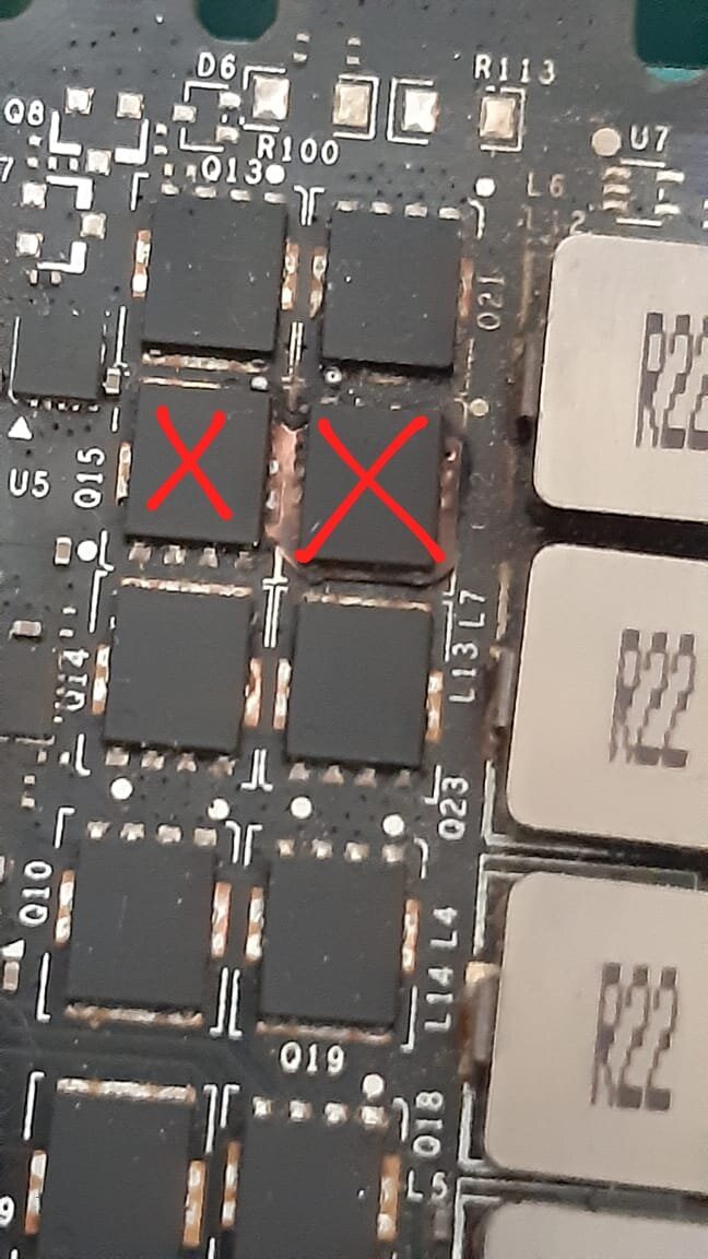  .jpg)
|
ty_ger07
Insert Custom Title Here

- Total Posts : 21174
- Reward points : 0
- Joined: 2008/04/10 23:48:15
- Location: traveler
- Status: offline
- Ribbons : 270

Re: GTX 970 FTW mosfet burnt
2021/05/08 06:13:05
(permalink)
4C10N is all you need. The code after it is manufacture location, manufacture date, and lot number. They won't match. Don't worry about that. Regarding the missing pad, that is a problem. The missing pad is the drain. It needs to be connected to wherever the drain connects. It is also a heatsink for the mosfet to dissipate heat into the PCB. Even if you reconnect the drain to wherever it comes from via a wire, without the pad to act as a heatsink, the new mosfet will likely not live long. If you are lucky, you can find where the drain connects, connect it with a wire, and then glue the new mosfet down to the pcb with thermal adhesive, and it may dissipate enough heat into the PCB to not burn up. Also, the burnt PCB is a problem. The burnt black stuff is carbon. It is electrically conductive. You have to carefully dig it all up, otherwise it will short out the inner layers. Then, you need to fill in the inner layers to keep them from shorting. Maybe that thermal adhesive would act as a good filler.
post edited by ty_ger07 - 2021/05/08 06:17:52
ASRock Z77 • Intel Core i7 3770K • EVGA GTX 1080 • Samsung 850 Pro • Seasonic PRIME 600W Titanium
My EVGA Score: 1546 • Zero Associates Points • I don't shill
|
xWinti
New Member
- Total Posts : 8
- Reward points : 0
- Joined: 2021/05/08 03:50:39
- Status: offline
- Ribbons : 0
Re: GTX 970 FTW mosfet burnt
2021/05/08 06:34:40
(permalink)
ty_ger07
4C10N is all you need. The code after it is manufacture location, manufacture date, and lot number. They won't match. Don't worry about that.
Regarding the missing pad, that is a problem. The missing pad is the drain. It needs to be connected to wherever the drain connects. It is also a heatsink for the mosfet to dissipate heat into the PCB. Even if you reconnect the drain to wherever it comes from via a wire, without the pad to act as a heatsink, the new mosfet will likely not live long. If you are lucky, you can find where the drain connects, connect it with a wire, and then glue the new mosfet down to the pcb with thermal adhesive, and it may dissipate enough heat into the PCB to not burn up.
Also, the burnt PCB is a problem. The burnt black stuff is carbon. It is electrically conductive. You have to carefully dig it all up, otherwise it will short out the inner layers. Then, you need to fill in the inner layers to keep them from shorting. Maybe that thermal adhesive would act as a good filler.
Clarification when you say thermal adhesive you mean thermal paste right? the same one used for cpu coolers, etc. So I removed the old mosfet and I carefully dug up the carbon and cleaned the place a bit with isopropyl alcohol. and this is how it looked like. You can see there's a black layer over the copper looking layer where the mosfet used to be, should I remove this black layer? And there's a hole as well. is this a good or a bad sign? And what should I do next? fill it up with thermal adhesive? 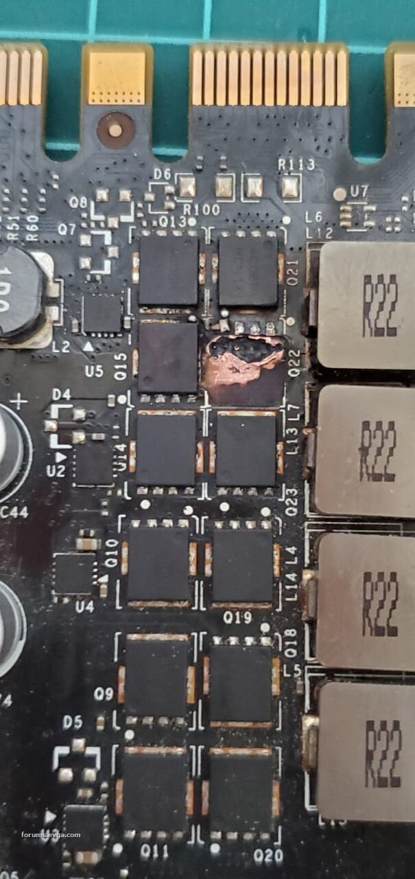
post edited by xWinti - 2021/05/08 07:24:04
Attached Image(s)
|
ty_ger07
Insert Custom Title Here
- Total Posts : 21174
- Reward points : 0
- Joined: 2008/04/10 23:48:15
- Location: traveler
- Status: offline
- Ribbons : 270
Re: GTX 970 FTW mosfet burnt
2021/05/08 10:53:53
(permalink)
No, not thermal paste. Thermal adhesive. Something which is rigid, would fill in the gaps, conducts heat, doesn't conduct electricity, and physically holds the part from moving. It is essentially like an epoxy that is good at conducting heat. I'll try to draw up a sketch of what I am envisioning. That latest picture is helpful. Can you please clarify one thing first?  I can't tell depth. Are those both the same copper layer, or did you expose an inner layer? I can't tell if you desoldered the old mostfet and folded that copper layer back down, or if that is a new copper layer which became exposed while cleaning out the charred PCB. It looks like they are separate layers, but I want to make sure.
post edited by ty_ger07 - 2021/05/08 11:16:50
ASRock Z77 • Intel Core i7 3770K • EVGA GTX 1080 • Samsung 850 Pro • Seasonic PRIME 600W Titanium
My EVGA Score: 1546 • Zero Associates Points • I don't shill
|
xWinti
New Member
- Total Posts : 8
- Reward points : 0
- Joined: 2021/05/08 03:50:39
- Status: offline
- Ribbons : 0
Re: GTX 970 FTW mosfet burnt
2021/05/08 15:12:42
(permalink)
ty_ger07
No, not thermal paste. Thermal adhesive. Something which is rigid, would fill in the gaps, conducts heat, doesn't conduct electricity, and physically holds the part from moving. It is essentially like an epoxy that is good at conducting heat.
I'll try to draw up a sketch of what I am envisioning. That latest picture is helpful.
Can you please clarify one thing first?
I can't tell depth. Are those both the same copper layer, or did you expose an inner layer? I can't tell if you desoldered the old mostfet and folded that copper layer back down, or if that is a new copper layer which became exposed while cleaning out the charred PCB.
It looks like they are separate layers, but I want to make sure.
they are seperate layers. When I desoldered the old mosfet the copper layer which was on top was stuck on the mosfet and it broke to pieces immediately. And then when i cleaned up the charred PCB this new copper layer became exposed.
|
ty_ger07
Insert Custom Title Here
- Total Posts : 21174
- Reward points : 0
- Joined: 2008/04/10 23:48:15
- Location: traveler
- Status: offline
- Ribbons : 270
Re: GTX 970 FTW mosfet burnt
2021/05/08 18:24:37
(permalink)
☄ Helpfulby xWinti 2021/05/09 02:47:47
ASRock Z77 • Intel Core i7 3770K • EVGA GTX 1080 • Samsung 850 Pro • Seasonic PRIME 600W Titanium
My EVGA Score: 1546 • Zero Associates Points • I don't shill
|
WindwalkerAlex
New Member
- Total Posts : 10
- Reward points : 0
- Joined: 2018/04/14 18:21:49
- Status: offline
- Ribbons : 0
Flagged as Spam (2)
Re: GTX 970 FTW mosfet burnt
2021/05/08 18:56:30
(permalink)
|
james1997bond
Superclocked Member

- Total Posts : 126
- Reward points : 0
- Joined: 2020/10/13 07:43:05
- Status: offline
- Ribbons : 0
Re: GTX 970 FTW mosfet burnt
2021/05/08 19:05:40
(permalink)
I had a 970 FTW die one recently after about 6 years. wondering if it's the same issue, I guess i'll have to tear it down. Were there any performance indiciations when this happened? For me, I would have random FPS dips. I also did oc the card for the first time in years and reapply thermal paste, so it could be that.
|
xWinti
New Member
- Total Posts : 8
- Reward points : 0
- Joined: 2021/05/08 03:50:39
- Status: offline
- Ribbons : 0
Re: GTX 970 FTW mosfet burnt
2021/05/09 04:51:32
(permalink)
ty_ger07
I don't have the card in front of me, so I am making my best guess that the two MOSFETs side-by-side have both of their drains connected together. I hope that is true.
With that assumption, this is what I would propose:


Alright, I'll try my best, and Ill update you on what happens with me next. Really appreciate the help man. Thanks a lot!
|
xWinti
New Member
- Total Posts : 8
- Reward points : 0
- Joined: 2021/05/08 03:50:39
- Status: offline
- Ribbons : 0
Re: GTX 970 FTW mosfet burnt
2021/05/09 04:54:29
(permalink)
james1997bond
I had a 970 FTW die one recently after about 6 years. wondering if it's the same issue, I guess i'll have to tear it down. Were there any performance indiciations when this happened? For me, I would have random FPS dips. I also did oc the card for the first time in years and reapply thermal paste, so it could be that.
Well, I think I mentioned in the beginning of the post that I bought this dead card to revive it. It wasn't working from the beginning. But regarding your card, I guess you could open your card and check for any physical damage at first. If you can't seem to find any physical damage, you could get a multimeter and use the continuity on the multimeter and diagnose your card. There are a lot of videos on YouTube that show how to diagnose the card and find the problem... Good luck!
|
james1997bond
Superclocked Member
- Total Posts : 126
- Reward points : 0
- Joined: 2020/10/13 07:43:05
- Status: offline
- Ribbons : 0
Re: GTX 970 FTW mosfet burnt
2021/05/09 09:22:26
(permalink)
Got it! I was just going to hang it up as a display but I suppose I'll try to diagnose it a little and see if i can get it working. Best of luck to your repairs!
|
ty_ger07
Insert Custom Title Here
- Total Posts : 21174
- Reward points : 0
- Joined: 2008/04/10 23:48:15
- Location: traveler
- Status: offline
- Ribbons : 270
Re: GTX 970 FTW mosfet burnt
2021/05/09 10:20:24
(permalink)
Adding to what I said earlier, again assuming that the drains of both Q15 and Q22 are supposed to be connected together (probably easier for you to determine than me), if both Q15 and Q22 are damaged (as indicated by the red X's that you provided), when you replace both Q15 and Q22, it might be best to solder down a thin copper layer under both Q15 and Q22 to provide better thermal transfer from Q22 to Q15, so that Q22 doesn't just burn up again right away. Q15 has intact vias below it to transfer heat to a PCB layer somewhere below. But Q22 will no longer have that connection since it will be sitting on top of epoxy. You could try filling the whole thing under Q22 with thermal adhesive instead of epoxy, for better thermal transfer to inner PCB layers, but I am not sure how easy it is to work with thermal adhesive, nor how well it behaves (both thermally and strength-wise) when applied in a thicker layer. Also, to clarify, I wouldn't recommend gluing the MOSFET to the copper layer (if you use one), but rather either glue the MOSFET directly to the PCB (or epoxy) OR solder the MOSFET to the coper layer which is then glued to the PCB (or epoxy). Additionally, another caution: Since (again) I don't own the card, it is impossible for me to know if you will have issues because you didn't connect Q22 to the vias below it (yellow circles in one of my images above). At least one of those vias might be part of a feedback circuit. Probably not, but it could be. I think that all of those vias are probably connected to a copper layer for thermal transfer which has no other electrical purpose, but I could be wrong. If you want to be absolutely sure, you could try to extend those vias up so that they make electrical contact with Q22, but good luck because it would make the repair and soldering a lot harder. Lastly, I have some additional concerns about a solder ball visible to the top right of Q15 and a solder ball visible to the bottom left of Q21, which could indicate more extensive PCB heat damage which is not currently visible. Worst case scenario, if the PCB is too damaged internally, assuming that the GPU core and/or memory didn't get spiked with 12 volts and is not already dead, if you can't get the VRM repair to work, you could just cut the VRM out completely, and solder on a different VRM power board (such as the EVGA EPOWER board). That mod wouldn't make economic sense, but depending on your goals, it would at least be an interesting learning experience.
post edited by ty_ger07 - 2021/05/09 12:48:09
ASRock Z77 • Intel Core i7 3770K • EVGA GTX 1080 • Samsung 850 Pro • Seasonic PRIME 600W Titanium
My EVGA Score: 1546 • Zero Associates Points • I don't shill
|
xWinti
New Member
- Total Posts : 8
- Reward points : 0
- Joined: 2021/05/08 03:50:39
- Status: offline
- Ribbons : 0
Re: GTX 970 FTW mosfet burnt
2021/05/09 15:28:03
(permalink)
I never noticed those two solder points you mentioned above. Fortunately I guess they just somehow ended up on the gpu. Because I just blew on them and they flew away and I checked under them where they were and there wasnt any sign of damage, so that's in the clear. Next, just to clarify, here's what Im going to do according to what you said... 1) Check that they're arent any connections touching each other. 2) Fill up the crater and the internal copper layer with some epoxy. 3) Glue a copper layer to the epoxy layer and then solder the mosfet Q22 on the copper layer and solder the mosfet connections to the board. Or optionally I could solder both Q15 and Q22 onto a copper layer since Q22 isnt connected to the vias. I hope this is how it should go. If not please feel free to correct me. Also I had one question, what are those solder connections exactly? 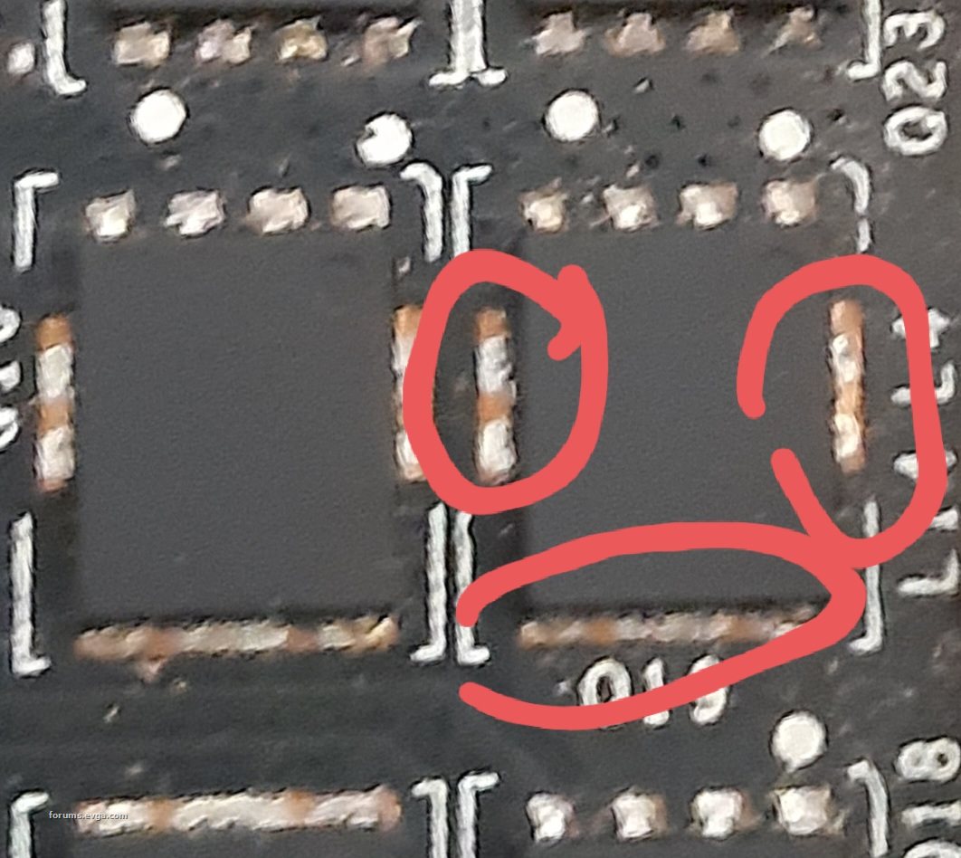 Lastly, thanks a bunch man for sticking with me and giving me a detailed guide and proposing really neat solutions while most other people on different forums just told me to throw the card in the trash. I really appreciate it. Even if the card doesnt work in the end, Im still happy from what Ive learned.
Attached Image(s)
|
ty_ger07
Insert Custom Title Here
- Total Posts : 21174
- Reward points : 0
- Joined: 2008/04/10 23:48:15
- Location: traveler
- Status: offline
- Ribbons : 270
Re: GTX 970 FTW mosfet burnt
2021/05/09 17:49:50
(permalink)
Those connections are for the drain of the MOSFET. If you look at the datasheet, you will see that about 3/4 of the back side is one big metal pad. It is all the drain. The exposed stubs on the side are just there so that you can put a soldering iron on them and get some heat on it, to make soldering and de-soldering using conventional techniques easier, instead of forcing you to have to use a hot air or oven reflow station. The drain is a big pad which connects the MOSFET to the PCB in a big area to give a lot of surface area for heat to soak into the PCB. The primary method to cool these MOSFETs is the PCB, and the thermal pad and heatsink on top just provides a fraction of the total MOSFET cooling. Trying to cool the MOSFET from the top with a thermal pad and heatsink isn't efficient since the top surface of the MOSFET isn't metal, and the thermal pad loses additional cooling efficiency. Picture from digikey:  When you solder it back together, remember to add plenty of flux. The flux core in the soldering wire is probably not enough. Flux makes everything a lot easier. I just dab a blob on with a q-tip and then solder over it. The flux keeps the solder from burning up and oxidizing right away (makes it less string-y/crystal-y), and makes the solder flow more where you want it to flow, and stay more where you want it to stay. It's like magic. Using Flux | Soldering Basics - YouTube Also, in case you weren't aware, this might be a lost cause. There is a possibility that when the MOSFET failed, it spiked the core or memory with 12 volts and the thing is dead dead no matter how hard you try and no matter how well you do.
post edited by ty_ger07 - 2021/05/09 22:37:34
ASRock Z77 • Intel Core i7 3770K • EVGA GTX 1080 • Samsung 850 Pro • Seasonic PRIME 600W Titanium
My EVGA Score: 1546 • Zero Associates Points • I don't shill
|
xWinti
New Member
- Total Posts : 8
- Reward points : 0
- Joined: 2021/05/08 03:50:39
- Status: offline
- Ribbons : 0
Re: GTX 970 FTW mosfet burnt
2021/05/11 12:46:33
(permalink)
Hey, I had a question where can I get the GPU circuit design?
|
ty_ger07
Insert Custom Title Here
- Total Posts : 21174
- Reward points : 0
- Joined: 2008/04/10 23:48:15
- Location: traveler
- Status: offline
- Ribbons : 270
Re: GTX 970 FTW mosfet burnt
2021/05/11 12:54:16
(permalink)
xWinti
Hey, I had a question where can I get the GPU circuit design?
Nowhere. You have to probe, research, reason, and sketch it out. Maybe someone else has already done a lot of that work, but I have no idea.
ASRock Z77 • Intel Core i7 3770K • EVGA GTX 1080 • Samsung 850 Pro • Seasonic PRIME 600W Titanium
My EVGA Score: 1546 • Zero Associates Points • I don't shill
|
james1997bond
Superclocked Member
- Total Posts : 126
- Reward points : 0
- Joined: 2020/10/13 07:43:05
- Status: offline
- Ribbons : 0
Re: GTX 970 FTW mosfet burnt
2021/05/12 10:22:33
(permalink)
Maybe call EVGA for it? Although it's probably highly proprietary and not something they might willingly share, they may be willing to in this case as it's an older card no longer in production.
|
ty_ger07
Insert Custom Title Here
- Total Posts : 21174
- Reward points : 0
- Joined: 2008/04/10 23:48:15
- Location: traveler
- Status: offline
- Ribbons : 270
Re: GTX 970 FTW mosfet burnt
2021/05/12 10:37:05
(permalink)
james1997bond
Maybe call EVGA for it? Although it's probably highly proprietary and not something they might willingly share, they may be willing to in this case as it's an older card no longer in production.
They won't.
ASRock Z77 • Intel Core i7 3770K • EVGA GTX 1080 • Samsung 850 Pro • Seasonic PRIME 600W Titanium
My EVGA Score: 1546 • Zero Associates Points • I don't shill
|
james1997bond
Superclocked Member
- Total Posts : 126
- Reward points : 0
- Joined: 2020/10/13 07:43:05
- Status: offline
- Ribbons : 0
Re: GTX 970 FTW mosfet burnt
2021/05/12 10:51:22
(permalink)
Yeah then no way you'll find it; there are just way too many components. I've never run across one over the years.
|
ty_ger07
Insert Custom Title Here
- Total Posts : 21174
- Reward points : 0
- Joined: 2008/04/10 23:48:15
- Location: traveler
- Status: offline
- Ribbons : 270
Re: GTX 970 FTW mosfet burnt
2021/05/21 22:36:44
(permalink)
ASRock Z77 • Intel Core i7 3770K • EVGA GTX 1080 • Samsung 850 Pro • Seasonic PRIME 600W Titanium
My EVGA Score: 1546 • Zero Associates Points • I don't shill
|
xWinti
New Member
- Total Posts : 8
- Reward points : 0
- Joined: 2021/05/08 03:50:39
- Status: offline
- Ribbons : 0
Re: GTX 970 FTW mosfet burnt
2021/05/22 06:03:36
(permalink)
I appreciate you keeping up with this man. Anyway, what happened is as follows..
I ordered the mosfet required "4C10N" and it arrived a couple days ago, my next step is to go to my university's digital logic design lab, because the engineer there agreed to help me to fix the issue following the steps that you provided me with. However, right now I'm having my semester finals (I study computer engineering), So I decided to work on it after I finish my finals on the 26th of May. When I'm done Ill let you know what happened with me.
|