kwkrnu72
SSC Member

- Total Posts : 598
- Reward points : 0
- Joined: 2012/11/28 14:54:55
- Status: offline
- Ribbons : 1

I know this relates to voltage regulation, and how the VRMs work. What I'm wondering is, what's the difference between 4+1, 6+2, 14+3? Is it more reliable, steady voltage? Do they allow for higher voltages? How does it work?
Aaaaand.....GO
|
kram36
The Destroyer

- Total Posts : 20362
- Reward points : 0
- Joined: 2009/10/27 19:00:58
- Location: United States
- Status: offline
- Ribbons : 72

Re: Explain "power phase"
2015/09/16 06:09:33
(permalink)
The more phases the "cleaner" the voltage is supplied and that's supposed to help with more stable over overclocking.
|
kwkrnu72
SSC Member

- Total Posts : 598
- Reward points : 0
- Joined: 2012/11/28 14:54:55
- Status: offline
- Ribbons : 1


Re: Explain "power phase"
2015/09/16 07:23:00
(permalink)
So, 6+1 or 14+3 isn't going to deliver MORE volts, just more steady voltage for more stable overclocking..... I wonder, though, if the better power phase will handle higher voltage better in terms of thermals?
|
Zuhl3156
Omnipotent Enthusiast

- Total Posts : 12765
- Reward points : 0
- Joined: 2010/03/23 12:52:50
- Location: Kidnapped by Gypsies
- Status: offline
- Ribbons : 34


Re: Explain "power phase"
2015/09/16 08:04:30
(permalink)
☄ Helpfulby kwkrnu72 2015/09/16 09:16:48
kwkrnu72
So, 6+1 or 14+3 isn't going to deliver MORE volts, just more steady voltage for more stable overclocking..... I wonder, though, if the better power phase will handle higher voltage better in terms of thermals?
This is the best explanation I found where it is compared to a car engine: http://www.techspot.com/community/topics/what-are-power-phases.169661/This is something I have been wondering about recently too since it was never explained to me but is getting more and more attention.
|
kwkrnu72
SSC Member

- Total Posts : 598
- Reward points : 0
- Joined: 2012/11/28 14:54:55
- Status: offline
- Ribbons : 1


Re: Explain "power phase"
2015/09/16 09:18:07
(permalink)
I'll read that tonight. My cards only have a 4+1 power phase, and I've been hesitant to push too much voltage through them thinking that it may harm them because they're not very "beefy". /shrug
|
kwkrnu72
SSC Member

- Total Posts : 598
- Reward points : 0
- Joined: 2012/11/28 14:54:55
- Status: offline
- Ribbons : 1


Re: Explain "power phase"
2015/09/16 12:19:04
(permalink)
Zuhl3156
kwkrnu72
So, 6+1 or 14+3 isn't going to deliver MORE volts, just more steady voltage for more stable overclocking..... I wonder, though, if the better power phase will handle higher voltage better in terms of thermals?
This is the best explanation I found where it is compared to a car engine: http://www.techspot.com/community/topics/what-are-power-phases.169661/
This is something I have been wondering about recently too since it was never explained to me but is getting more and more attention.
I read through that on my lunch break. That's the best explanation I've seen thus far, but it still leaves me wanting more. It didn't really satisfy my curious nature. = P
|
Tweaked
CLASSIFIED ULTRA Member

- Total Posts : 6505
- Reward points : 0
- Joined: 2006/08/12 12:24:15
- Location: Texas
- Status: offline
- Ribbons : 29

Re: Explain "power phase"
2015/09/16 12:37:53
(permalink)
☼ Best Answerby kwkrnu72 2015/09/16 14:34:23
I'll do my best to explain. As you probably know, electricity travels in waves. This is called alternating current. Each wave has a peak and a trough. The peak is known as the positive cycle and the trough is the negative as referenced by a mid point between them. The negative cycle is 180 degrees out of phase with the positive cycle so that it looks like this. 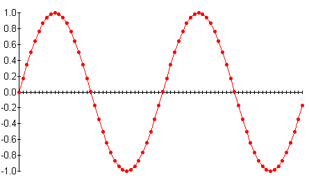 Notice the enormous gap between the two positive cycles. This causes power fluctuations. To compensate for this, more phases of power are introduced in between those positive cycles to try and smooth it out so that it looks like this.  Now notice that the distance between each peak of the positive cycle is smaller and that the power begins to rise again before it reaches the negative cycle or trough of the first phase and then the second phase. As you continue to add more phases of power, the amount of distance between positive peaks continues to be reduced resulting in a more constant, steady stream of power to your device and more stability of operation.

 EVGA DG-77/ EVGA 750 G2/ Gigabyte B450/ AMD Ryzen 5 3600/ 16gb Crucial Ballistix DDR4-3600/ RTX-2080 XC/ Dell S2716DG / Windows 11 64
|
Sajin
EVGA Forum Moderator

- Total Posts : 49219
- Reward points : 0
- Joined: 2010/06/07 21:11:51
- Location: Texas, USA.
- Status: online
- Ribbons : 199


Re: Explain "power phase"
2015/09/16 13:46:43
(permalink)
Pretty simple...
More phases = cleaner & more constant power delivered to gpu which = better stability and better overclocking results. Cards like the classy and kingpin can push more volts than reference cards due to the way the vrm is designed.
|
kwkrnu72
SSC Member

- Total Posts : 598
- Reward points : 0
- Joined: 2012/11/28 14:54:55
- Status: offline
- Ribbons : 1


Re: Explain "power phase"
2015/09/16 13:54:26
(permalink)
So the voltage delivery is a lot more stable, and since there are more VRMs then the temps are probably a tad lower.
Come to find out....doesn't matter on my cards, my cards have a hardware cap of 1.275v....no danger of hurting ANYTHING at that voltage.
|
kwkrnu72
SSC Member

- Total Posts : 598
- Reward points : 0
- Joined: 2012/11/28 14:54:55
- Status: offline
- Ribbons : 1


Re: Explain "power phase"
2015/09/16 14:34:52
(permalink)
I really appreciate the help, gents. Thank you!
|
TECH_DaveB
EVGA Alumni

- Total Posts : 4661
- Reward points : 0
- Joined: 2008/09/26 17:03:47
- Status: offline
- Ribbons : 46

Re: Explain "power phase"
2015/09/16 15:40:42
(permalink)
Glad you got it figured out.
Tweaked directed you right on this, I have known him personally for several years, guy knows his stuff and is pretty darned helpful. Want to really get techy, start asking him about high end audio :)
|
ManBearPig
CLASSIFIED ULTRA Member

- Total Posts : 5116
- Reward points : 0
- Joined: 2007/10/31 12:02:13
- Location: Imaginationland
- Status: offline
- Ribbons : 20


Re: Explain "power phase"
2015/09/16 15:48:33
(permalink)
Wow, thanks Tweaked. All I knew was the more you had, the cleaner and more stable the power was. Good to know the actual explanation 
|
un4givn85
SSC Member

- Total Posts : 903
- Reward points : 0
- Joined: 2011/02/01 14:35:34
- Location: MT
- Status: offline
- Ribbons : 1


Re: Explain "power phase"
2015/09/16 19:26:46
(permalink)
So what does the +1 mean? Why not just call it 5 instead of 4+1?
|
kwkrnu72
SSC Member

- Total Posts : 598
- Reward points : 0
- Joined: 2012/11/28 14:54:55
- Status: offline
- Ribbons : 1


Re: Explain "power phase"
2015/09/16 19:27:17
(permalink)
Yeah...that explanation was exactly what I was looking for.
|
Tweaked
CLASSIFIED ULTRA Member

- Total Posts : 6505
- Reward points : 0
- Joined: 2006/08/12 12:24:15
- Location: Texas
- Status: offline
- Ribbons : 29

Re: Explain "power phase"
2015/09/16 19:52:23
(permalink)
un4givn85
So what does the +1 mean? Why not just call it 5 instead of 4+1?
Because that portion of the power is shunted to the memory controller as explained in this excerpt from the above link.
The +2 part of the equation (8+2, 12+2 etc.) refers to the same principle, but in this instance the current is going to the memory controller (either chipset, or in the CPU if the controller is part of the CPU package).
So, 8 or 12 phases go one direction, and 2 phases go another. It delineates how many phases of power go to which components on the motherboard.

 EVGA DG-77/ EVGA 750 G2/ Gigabyte B450/ AMD Ryzen 5 3600/ 16gb Crucial Ballistix DDR4-3600/ RTX-2080 XC/ Dell S2716DG / Windows 11 64
|
un4givn85
SSC Member

- Total Posts : 903
- Reward points : 0
- Joined: 2011/02/01 14:35:34
- Location: MT
- Status: offline
- Ribbons : 1


Re: Explain "power phase"
2015/09/16 19:53:31
(permalink)
Tweaked
un4givn85
So what does the +1 mean? Why not just call it 5 instead of 4+1?
Because that portion of the power is shunted to the memory controller as explained in this excerpt from the above link.
The +2 part of the equation (8+2, 12+2 etc.) refers to the same principle, but in this instance the current is going to the memory controller (either chipset, or in the CPU if the controller is part of the CPU package).
So, 8 or 12 phases go one direction, and 2 phases go another. It delineates how many phases of power go to which components on the motherboard.
Thank you.
|
ty_ger07
Insert Custom Title Here

- Total Posts : 16601
- Reward points : 0
- Joined: 2008/04/10 23:48:15
- Location: traveler
- Status: offline
- Ribbons : 271


Re: Explain "power phase"
2015/09/16 20:35:19
(permalink)
☄ Helpfulby kwkrnu72 2015/09/17 06:33:32
I highlighted a number of things for you. I hope this helps: 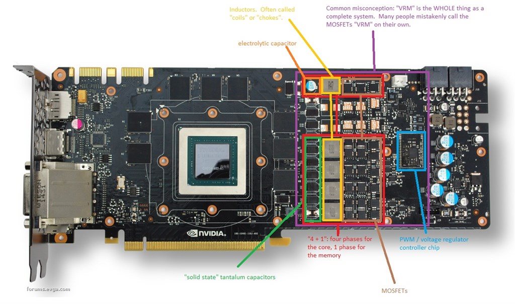 First of all, I would like to clear up something which has been made a little bit misleading. The increased number of power phases do not necessarily smooth out the voltage output. The image posted by tweaked is very misleading because that is not what the voltage ouput looks like. ... Not even close! If you look at his first picture with a single phase and compare it to his second picture with three phases, you may think that of coarse it looks smoother with three phases. This is not necessarily the case! The output is filtered by the inductors and capacitors. It is a DC to DC buck converter system and the output voltage is not anywhere even close to a sine wave at the end. There actually is no sine wave in this whole system to begin with -- because it is a square wave and the square wave only exists from the voltage regulator up to and through the MOSFETs. After the square wave output of the MOSFETs, the inductors and capacitors filter the square wave and their output should be nearly ripple-free and look like normal DC and will not ever look anything even close to the AC represented in tweaked's illustrations. Below is the output from an actual buck converter. The two sawtooth waves at the bottom are the two different phases read after the inductors (before the capacitors). The inductors chew the sharp edges off the square waves fed to them by adsorbing the harmonics which constitute a square wave's corners. Then, after the capacitors smooth out the sawtooth waves, you see the top two waves as the DC output with some ripple. The ripple will tend to even out as more and more phases are added together, but it isn't nearly as bad as initially illustrated and the ripple is only a tiny fluctuation way above the zero plane -- not a huge oscillation about the zero plane.  As you can see in the illustration above, their device put out 10 volts DC with about 0.010 volts of ripple per phase. 1/1000th defect. This was only an example of real-world observation. More phases may equate to smoother power delivery. Also, more phases may equate to higher current capability. But buyer beware!! Just like cheap computer manufacturerers sometime sell an excessive quantity of cheap low performance memory in their product because some buyers don't know any better and think that more memory means a faster computer, some video card and motherboard manufacturers are exploiting similar tactics regarding power phases. Fewer power phases coupled with well engineered filtering in the inductor/capacitor section can be much better than a bunch of power phases tossed on a product with poor engineering. Additionally, the voltage regulator controller chip is very important both in maintaining desired voltage output and in determining whether or not the user can easily interract with their product in terms of changing voltages. The voltage controller chip may not be adjustable by the user at all, may be adjustable only through proprietary methods with strict limits, or may be adjustable openly using industry standard SMBus or I-squared-C, and may even allow for adjustment of the output PWM frequency. Cheap products with lots of phases are just cheap products with lots of phases. All the individual components illustrated in the picture above need to be chosen carefully in order to match together in a great product. Lastly, one should remember that if one does not need additional power phases, one should consider avoiding additional power phases if performance per watt and heat output are crucial factors in their system component choices. But, if you really want to maximize your potential and aren't worried about the reduced efficiency and increased cost, it is hard to beat a product with a bunch of very well engineered power phases coupled with a voltage controller chip which is easily accessible and tunable.
post edited by ty_ger07 - 2015/09/16 23:31:59
Attached Image(s)
|
Tweaked
CLASSIFIED ULTRA Member

- Total Posts : 6505
- Reward points : 0
- Joined: 2006/08/12 12:24:15
- Location: Texas
- Status: offline
- Ribbons : 29

Re: Explain "power phase"
2015/09/16 21:37:57
(permalink)
ty_ger07
I highlighted a number of things for you. I hope this helps:

First of all, I would like to clear up something which has been made a little bit misleading. The increased number of power phases do not necessarily smooth out the voltage output. The image posted by tweaked is very misleading because that is not what the voltage ouput looks like. ... Not even close! If you look at his first picture with a single phase and compare it to his second picture with three phases, you may think that of coarse it looks smoother with three phases. This is not necessarily the case! The output is filtered by the inductors and capacitors. It is a DC to DC buck converter system and the output voltage is not anywhere even close to a sine wave at the end. There actually is no sine wave in this whole system to begin with -- because it is a square wave and the square wave only exists from the voltage regulator up to and through the MOSFETs. After the square wave output of the MOSFETs, the inductors and capacitors filter the square wave and their output should be nearly ripple-free and look like normal DC and will not ever look anything even close to the AC represented in tweaked's illustrations.
More phases may equate to smoother power delivery. Also, more phases may equate to higher current capability. But buyer beware!! Just like cheap computer manufacturerers sometime sell an excessive quantity of cheap low performance memory in their product because some buyers don't know any better and think that more memory means a faster computer, some video card and motherboard manufacturers are exploiting similar tactics regarding power phases.
Fewer power phases coupled with well engineered filtering in the inductor/capacitor section can be much better than a bunch of power phases tossed on a product with poor engineering. Additionally, the voltage regulator controller chip is very important both in maintaining desired voltage output and in determining whether or not the user can easily interract with their product in terms of changing voltages. The voltage controller chip may not be adjustable by the user at all, may be adjustable only through proprietary methods with strict limits, or may be adjustable openly using industry standard SMBus or I-squared-C, and may even allow for adjustment of the output PWM frequency. Cheap products with lots of phases are just cheap products with lots of phases. All the individual components illustrated in the picture above need to be chosen carefully in order to match together in a great product.
Lastly, one should remember that if one does not need additional power phases, one should consider avoiding additional power phases if performance per watt and heat output are crucial factors in their system component choices. But, if you really want to maximize your potential and aren't worried about the reduced efficiency and increased cost, it is hard to beat a product with a bunch of very well engineered power phases coupled with a voltage controller chip which is easily accessible and tunable.
Well, what can I say. Thank you for correcting me and clarifying this for all of us.

 EVGA DG-77/ EVGA 750 G2/ Gigabyte B450/ AMD Ryzen 5 3600/ 16gb Crucial Ballistix DDR4-3600/ RTX-2080 XC/ Dell S2716DG / Windows 11 64
|
kwkrnu72
SSC Member

- Total Posts : 598
- Reward points : 0
- Joined: 2012/11/28 14:54:55
- Status: offline
- Ribbons : 1


Re: Explain "power phase"
2015/09/17 06:36:21
(permalink)
All things being equal, and knowing that EVGA usually used high quality pieces, I don't think that the "low quality" part is really an issue. Great information though, thank you for the post!
|
ty_ger07
Insert Custom Title Here

- Total Posts : 16601
- Reward points : 0
- Joined: 2008/04/10 23:48:15
- Location: traveler
- Status: offline
- Ribbons : 271


Re: Explain "power phase"
2015/09/20 18:13:40
(permalink)
EVGA does usually use high quality components, yes. Their components are up to NVIDIA reference standards or better. On their reference boards, the VRM can be rather lackluster in some cases for cost cutting reasons (NVIDIA's reference GTX 285 second revision for example which was created for cost cutting which EVGA also sold), but on their custom products with suped up VRM, better, yes. I hope that my biggest points were still helpful: 1) In general, don't assume that more phases are better. EVGA has made good products (equal to or better than NVIDIA reference standard) and tend to advertise honestly (in my opinion), but don't assume that it is true for all manufacturers nor assume that it will be true forever. 2) Realize that the voltage ripple in the VRM output may only be 0.1% (for example) in a standard product and don't assume that another more expensive version with 0.05% voltage ripple will behave very differently. 3) If performance per watt and thermal efficiency are extremely important in your system, extra phases will probably be a drawback.
post edited by ty_ger07 - 2015/09/20 18:19:30
|
kwkrnu72
SSC Member

- Total Posts : 598
- Reward points : 0
- Joined: 2012/11/28 14:54:55
- Status: offline
- Ribbons : 1


Re: Explain "power phase"
2015/09/20 18:29:14
(permalink)
I would prefer the highest performance possible, regardless of how efficient it is. I took a card that is set up to run at 170 watts / 187 watts and have it pulling over 280....don't much care about efficiency. = ) lol
|
willem445
CLASSIFIED Member

- Total Posts : 4184
- Reward points : 0
- Joined: 2010/05/25 17:30:49
- Status: offline
- Ribbons : 13


Re: Explain "power phase"
2016/06/06 09:09:51
(permalink)
☄ Helpfulby Cool GTX 2019/03/09 16:37:44
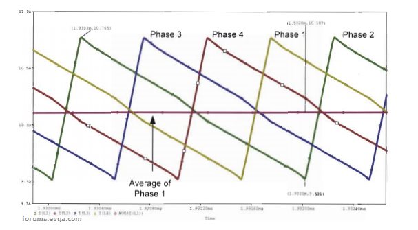
I know this is an old thread but I wanted to clarify some things in case anyone else stumbles across this thread as I did. I saw a thread about the Zotac GTX 1080 showing a large number of power phases on the PCB, which got me wondering, what exactly are these phases. Being an EE student, power electronics interest me so I looked into it. The pictures Tweaked referenced are extremely misleading. The second picture just illustrates 3 phase power, what the US power transmission system consists of, 3 120VAC phases and a common. The first image is just one of those 3 phases, which is what you would see at an electrical outlet. The PSU converts the 120VAC to 12VDC so the GPU never sees anything close to AC power. The phases of the GPU power system are just multiple DC-DC buck converters. The purpose of the buck converters is to reduce the 12VDC down to whatever the GPU die requires, around 1V. Now the design of DC-DC converters is difficult for voltages around 1 volt. You have to deal with efficiency, duty cycle, switching frequency, etc which all work against each other. Anyways, for such small voltages, the die requires massive currents. If the voltage conversion was done in just one stage, you would need much larger inductors and smoothing capacitors to handle the large current and voltage ripple requirements of the GPU. Efficiency also suffers here. When more phases are added to the buck converter system, the load on the FETs and inductor is greatly decreased. This reduces the inductor size required, reduces power losses across the inductors and FETs increasing power efficiency, this also helps immensely in spreading the heat evenly, reducing thermal hotspots. Current ripple is also improved also lowering voltage ripple. So with more phases, such as on classified cards, the converters can handle the increased current requirements seen with overclocking and help spread the increased heat more evenly while also reducing ripple at the input to the GPU die. EDIT: A bit more explanation on how it actually works. So PWM controller "clocks" each mosfet gate of each phase separately with dead time between each "clock" to avoid unwanted transient behavior. Here is what the waveform would look like. 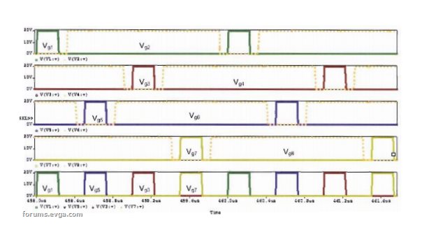 This causes the current ripple at the output of each phase to be out of phase with each other. This is a good thing since when all of the phases are averaged, the current ripple is almost completely canceled out. Since current and voltage are directly related, the voltage ripple is also greatly reduced. Each phase handles much less current then if a single phase was used. The currents are summed at the output of the converter and routed to the GPU die.  Ty_ger07's explanation is very good but lacked some of the more technical details. He is also correct in that the quality of components is also very important. Special components help to further reduce losses and increase efficiency while also lasting longer. I wouldn't doubt that EVGA uses high quality components as their cards have always performed very well. I hope my explanation makes sense and helps out people who are curious about phases as well. Feel free to correct me if I have made any mistakes. It would be very interesting to actually see a schematic of one of these cards to see how they accomplish power delivery. A great deal of this information came from reading this article as well as the pictures. A good read from a technical standpoint. Shows the 4 phase design process. http://digitalcommons.calpoly.edu/cgi/viewcontent.cgi?article=1030&context=theses Also found this based on an IC found on a high resolution photo of an ASUS GTX 980. The data sheet shows the common configuration for 8 phase power control if anyone is interested. http://www.infineon.com/d...3600a40153567f4b2128a4
post edited by willem445 - 2016/06/07 06:01:08
Attached Image(s)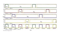 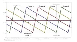
|
kgrames
New Member

- Total Posts : 6
- Reward points : 0
- Joined: 2016/05/27 21:36:18
- Status: offline
- Ribbons : 0

Re: Explain "power phase"
2016/06/06 19:02:24
(permalink)
willem445
I know this is an old thread but I wanted to clarify some things in case anyone else stumbles across this thread as I did. I saw a thread about the Zotac GTX 1080 showing a large number of power phases on the PCB, which got me wondering, what exactly are these phases. Being an EE student, power electronics interest me so I looked into it.
The pictures Tweaked referenced are extremely misleading. The second picture just illustrates 3 phase power, what the US power transmission system consists of, 3 120VAC phases and a common. The first image is just one of those 3 phases, which is what you would see at an electrical outlet. The PSU converts the 120VAC to 12VDC so the GPU never sees anything close to AC power. The phases of the GPU power system are just multiple DC-DC buck converters. The purpose of the buck converters is to reduce the 12VDC down to whatever the GPU die requires, around 1V. Now the design of DC-DC converters is difficult for voltages around 1 volt. You have to deal with efficiency, duty cycle, switching frequency, etc which all work against each other.
Anyways, for such small voltages, the die requires massive currents. If the voltage conversion was done in just one stage, you would need much larger inductors and smoothing capacitors to handle the large current and voltage ripple requirements of the GPU. Efficiency also suffers here. When more phases are added to the buck converter system, the load on the FETs and inductor is greatly decreased. This reduces the inductor size required, reduces power losses across the inductors and FETs increasing power efficiency, this also helps immensely in spreading the heat evenly, reducing thermal hotspots. Current ripple is also improved also lowering voltage ripple. So with more phases, such as on classified cards, the converters can handle the increased current requirements seen with overclocking and help spread the increased heat more evenly while also reducing ripple at the input to the GPU die.
Ty_ger07's explanation is very good but lacked some of the more technical details. He is also correct in that the quality of components is also very important. Special components help to further reduce losses and increase efficiency while also lasting longer. I wouldn't doubt that EVGA uses high quality components as their cards have always performed very well.
I hope my explanation makes sense and helps out people who are curious about phases as well. Feel free to correct me if I have made any mistakes. It would be very interesting to actually see a schematic of one of these cards to see how they accomplish power delivery.
Also found this based on an IC found on a high resolution photo of an ASUS GTX 980. The data sheet shows the common configuration for 8 phase power control if anyone is interested.
Great explanation!
|
willem445
CLASSIFIED Member

- Total Posts : 4184
- Reward points : 0
- Joined: 2010/05/25 17:30:49
- Status: offline
- Ribbons : 13


Re: Explain "power phase"
2016/06/07 06:06:12
(permalink)
kgrames
willem445
I know this is an old thread but I wanted to clarify some things in case anyone else stumbles across this thread as I did. I saw a thread about the Zotac GTX 1080 showing a large number of power phases on the PCB, which got me wondering, what exactly are these phases. Being an EE student, power electronics interest me so I looked into it.
The pictures Tweaked referenced are extremely misleading. The second picture just illustrates 3 phase power, what the US power transmission system consists of, 3 120VAC phases and a common. The first image is just one of those 3 phases, which is what you would see at an electrical outlet. The PSU converts the 120VAC to 12VDC so the GPU never sees anything close to AC power. The phases of the GPU power system are just multiple DC-DC buck converters. The purpose of the buck converters is to reduce the 12VDC down to whatever the GPU die requires, around 1V. Now the design of DC-DC converters is difficult for voltages around 1 volt. You have to deal with efficiency, duty cycle, switching frequency, etc which all work against each other.
Anyways, for such small voltages, the die requires massive currents. If the voltage conversion was done in just one stage, you would need much larger inductors and smoothing capacitors to handle the large current and voltage ripple requirements of the GPU. Efficiency also suffers here. When more phases are added to the buck converter system, the load on the FETs and inductor is greatly decreased. This reduces the inductor size required, reduces power losses across the inductors and FETs increasing power efficiency, this also helps immensely in spreading the heat evenly, reducing thermal hotspots. Current ripple is also improved also lowering voltage ripple. So with more phases, such as on classified cards, the converters can handle the increased current requirements seen with overclocking and help spread the increased heat more evenly while also reducing ripple at the input to the GPU die.
Ty_ger07's explanation is very good but lacked some of the more technical details. He is also correct in that the quality of components is also very important. Special components help to further reduce losses and increase efficiency while also lasting longer. I wouldn't doubt that EVGA uses high quality components as their cards have always performed very well.
I hope my explanation makes sense and helps out people who are curious about phases as well. Feel free to correct me if I have made any mistakes. It would be very interesting to actually see a schematic of one of these cards to see how they accomplish power delivery.
Also found this based on an IC found on a high resolution photo of an ASUS GTX 980. The data sheet shows the common configuration for 8 phase power control if anyone is interested.
Great explanation!
Thanks! Added a bit more information as well.
|
xeryx
New Member

- Total Posts : 1
- Reward points : 0
- Joined: 2016/07/01 11:47:47
- Status: offline
- Ribbons : 0

Re: Explain "power phase"
2016/07/01 12:08:52
(permalink)
willem445
I know this is an old thread but I wanted to clarify some things in case anyone else stumbles across this thread as I did. I saw a thread about the Zotac GTX 1080 showing a large number of power phases on the PCB, which got me wondering, what exactly are these phases. Being an EE student, power electronics interest me so I looked into it.
The pictures Tweaked referenced are extremely misleading. The second picture just illustrates 3 phase power, what the US power transmission system consists of, 3 120VAC phases and a common. The first image is just one of those 3 phases, which is what you would see at an electrical outlet. The PSU converts the 120VAC to 12VDC so the GPU never sees anything close to AC power. The phases of the GPU power system are just multiple DC-DC buck converters. The purpose of the buck converters is to reduce the 12VDC down to whatever the GPU die requires, around 1V. Now the design of DC-DC converters is difficult for voltages around 1 volt. You have to deal with efficiency, duty cycle, switching frequency, etc which all work against each other.
Anyways, for such small voltages, the die requires massive currents. If the voltage conversion was done in just one stage, you would need much larger inductors and smoothing capacitors to handle the large current and voltage ripple requirements of the GPU. Efficiency also suffers here. When more phases are added to the buck converter system, the load on the FETs and inductor is greatly decreased. This reduces the inductor size required, reduces power losses across the inductors and FETs increasing power efficiency, this also helps immensely in spreading the heat evenly, reducing thermal hotspots. Current ripple is also improved also lowering voltage ripple. So with more phases, such as on classified cards, the converters can handle the increased current requirements seen with overclocking and help spread the increased heat more evenly while also reducing ripple at the input to the GPU die.
EDIT: A bit more explanation on how it actually works.
So PWM controller "clocks" each mosfet gate of each phase separately with dead time between each "clock" to avoid unwanted transient behavior. Here is what the waveform would look like.

This causes the current ripple at the output of each phase to be out of phase with each other. This is a good thing since when all of the phases are averaged, the current ripple is almost completely canceled out. Since current and voltage are directly related, the voltage ripple is also greatly reduced. Each phase handles much less current then if a single phase was used. The currents are summed at the output of the converter and routed to the GPU die.
Ty_ger07's explanation is very good but lacked some of the more technical details. He is also correct in that the quality of components is also very important. Special components help to further reduce losses and increase efficiency while also lasting longer. I wouldn't doubt that EVGA uses high quality components as their cards have always performed very well.
I hope my explanation makes sense and helps out people who are curious about phases as well. Feel free to correct me if I have made any mistakes. It would be very interesting to actually see a schematic of one of these cards to see how they accomplish power delivery.
A great deal of this information came from reading this article as well as the pictures. A good read from a technical standpoint. Shows the 4 phase design process.
Also found this based on an IC found on a high resolution photo of an ASUS GTX 980. The data sheet shows the common configuration for 8 phase power control if anyone is interested.
Great Job on your explanation on the power phases. The one thing that you did forget to explain however is the Wattage! and how it affects the card. So I will try and fill in the blanks as simply as possible. Most GPUs and CPU's have a Mosfet and VRM system of at least 4 phases. Each time a vrm turns on is a time it draws current and heats up. Being able to split this time between 10 VRMS allows for the non firing VRMS to have a chance to cool down. This allows for a much more even temperature generation over the components, this in turn also allows the heat sinks (it is UBER important to look at heat sink design, and EVGA has amongst the best I have seen) to be able to effectively dissipate the heat. HEAT = Watts and Increase in Watts is proportional to increase in current draw. The faster you push your components the more current is drawn..think of current like the gasoline feeding the 8 cylinder (Vrms and mosfets). When you race your "engine" it generates much more heat, than when it is just cruising though town. HEAT is a major factor in preventing high overclocks, if it cannot be dissipated efficiently you will not be able to overclock much regardless of how many phases of power you have! The two are engineered hand in hand. Like a car You have to be able to cool your engine, and that is why the cooling solution is so important. That is all I will say on that
|