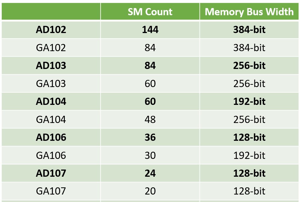
https://www.techpowerup.com/292555/nvidia-geforce-ada-lovelace-memory-bus-width-info-leaked The deluge of NVIDIA leaks continue following the major cyber-attack on the company, with hackers getting away with sensitive information about current and upcoming products. The latest in this series covers the memory bus widths of the next-generation RTX 40-series GPUs based on the "Ada Lovelace" graphics architecture. There is early-information covering the streaming multiprocessor (SM) counts of each GPU, and their large on-die caches.
The top-of-the-line AD102 silicon allegedly has a 384-bit wide memory bus, similar to its predecessor. The next-best AD103 silicon has a 256-bit wide memory bus. Things get very interesting with the AD104, which has a 192-bit wide memory bus. The AD104 is a revelation here, because it succeeds a long line of NVIDIA GPUs with 256-bit memory buses (eg: GA104, TU104, GP104, GM204, etc). This confirms the theory that much like AMD, NVIDIA is narrowing the memory bus widths in the lower segments to cut board costs, and compensate for the narrower bus-width with large on-die caches, high memory data-rates, and other memory-management optimizations.
Keeping with the theme we described above, the AD106 is expected to feature a 128-bit wide bus, while its predecessors, the GA106 and TU106, have 192-bit. Interestingly, NVIDIA didn't cheap out with bus-width on its smallest AD107 chip, which continues to have 128-bit bus width. We expect NVIDIA to use faster memory data-rates across the board. For the lower-end, the company could tap into 16 Gbps chips if they are priced right, and bring GDDR6X to the performance segment.
The upper level models seem to have increased bus width.
