Intel "Alder Lake" Silicon Variants Detailed | TechPowerUp The 12th Gen Core "Alder Lake" microarchitecture will see Intel unify its desktop- and mobile processor IP, back to the way things were up to the 9th Gen. With its post-14 nm silicon fabrication nodes in their infancy, Intel had diverged the client processor IP across its 10th and 11th Gen Core. With 10th Gen, the company introduced "Ice Lake" for ultra-portable platforms (28 W and below), while retaining 14 nm "Comet Lake" for mainstream notebooks (28 W to 45 W); while keeping desktop exclusively with 14 nm "Comet Lake." For 11th Gen, the story is mostly similar. Cutting-edge 10 nm "Tiger Lake" now covers all mobile categories, while desktop receives an IPC upgrade, thanks to the 14 nm "Rocket Lake." The 12th Gen will see a common microarchitecture, "Alder Lake," span across all client segments, from 7 W ultra mobile, to 125 W enthusiast desktop.
This, however, doesn't mean that Intel has a one-size fits all silicon that it can carve SKUs out of. The company has developed as many as three physical dies based on "Alder Lake," which vary in CPU core counts, the size of the iGPU, and other on-die components. "Alder Lake" is a hybrid processor with a combination of larger "Golden Cove" P-cores, and smaller "Gracemont" E-cores. The P-cores are spatially large, and along with their L3 cache slices, take up a large share of the compute portion of the silicon. The E-cores come in clusters of 4 cores each.
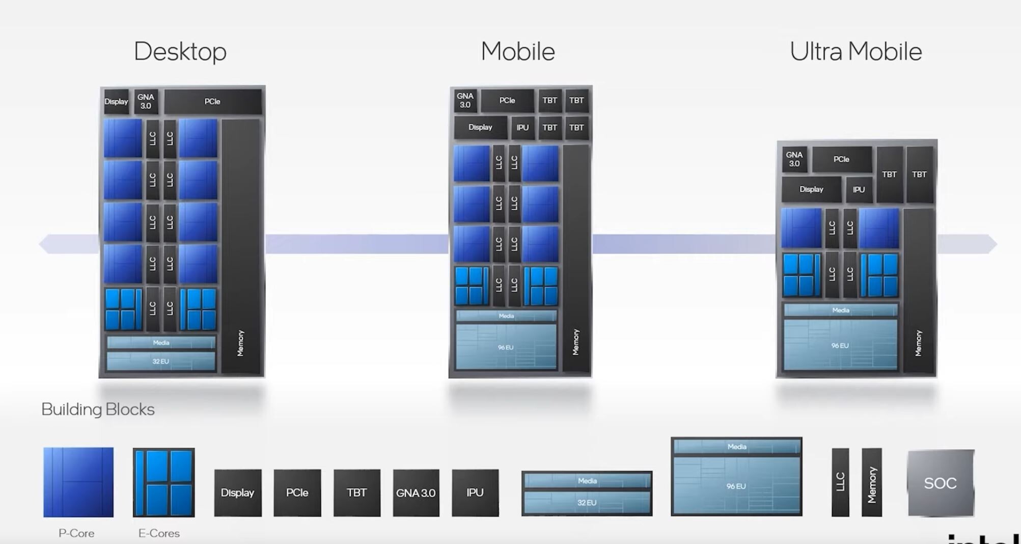
The desktop segment, headed by the new LGA1700 socket, receives the largest die. Physically, it has 8 P-cores, and 8 E-cores across two clusters. The chip also features the smallest iGPU, with only 32 execution units. Being a desktop platform, the iGPU enjoys much greater power budget and can run at higher clock speeds to try and make up for the lower EU count. A larger 28-32 lane PCI-Express Gen 5 root complex, and a dual-channel DDR5 memory interface, make for the rest of this die. GNA 3.0, or Gaussian Network Accelerator, a hardware component required for DLBoost to work, also makes its presence felt.
A slightly smaller silicon, targeting mobile platforms in the 28 W to 45 W (or beyond) range, is designed for the BGA Type 3 package (which measures 50 mm x 25 mm x 1.3 mm). This die physically has 6 P-cores, 8 E-cores across two clusters, a dual-channel DDR5 + LPDDR5 memory interface, and a PCI-Express Gen 5 root complex (albeit with fewer lanes than the "Alder Lake-S" desktop silicon). The chip has a much larger Xe LP-based iGPU with 96 execution units, and four integrated Thunderbolt 4 controllers.
The smallest of the three dies targets ultra-portable platforms in the 7 W to 28 W category, and comes in the tiny BGA type-4 package measuring 28.5 mm x 19 mm x 1.1 mm. This silicon physically only has 2 P-cores, but all 8 E-cores, the larger 96-EU iGPU, two integrated Thunderbolt 4 interfaces, and the same narrower PCI-Express Gen 5 interface. Memory remains the same, with support for both DDR5 and LPDDR5.
Both the BGA type-3 and BGA type-4 packages are multi-chip modules, with the processor die and the PCH die. The processor die talks to the PCH over EMIB. The desktop "Alder Lake-S," however, is a conventional 2-chip solution, with the PCH on the motherboard.
All variants of "Alder Lake" silicon are built on the Intel 7 process, which was formerly known as 10 nm Enhanced SuperFin.
Having the architecture across desktop and mobile should help to cut costs in my opinion.
