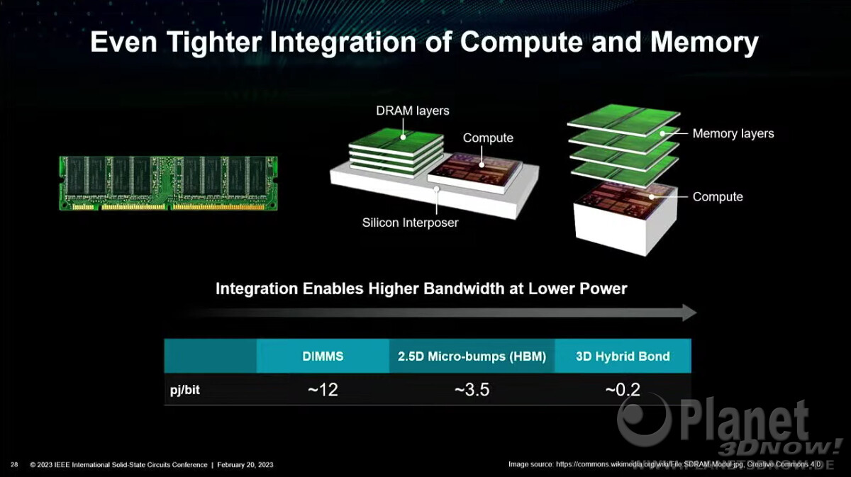
https://www.techpowerup.com/305060/amd-envisions-stacked-dram-on-top-of-compute-chiplets-in-the-near-future AMD in its ISSCC 2023 presentation detailed how it has advanced data-center energy-efficiency and managed to keep up with Moore's Law, even as semiconductor foundry node advances have tapered. Perhaps its most striking prediction for server processors and HPC accelerators is multi-layer stacked DRAM. The company has, for some time now, made logic products, such as GPUs, with stacked HBM. These have been multi-chip modules (MCMs), in which the logic die and HBM stacks sit on top of a silicon interposer. While this conserves PCB real-estate compared to discrete memory chips/modules; it is inefficient on the substrate, and the interposer is essentially a silicon die that has microscopic wiring between the chips stacked on top of it.
AMD envisions that the high-density server processor of the near-future will have many layers of DRAM stacked on top of logic chips. Such a method of stacking conserves both PCB and substrate real-estate, allowing chip-designers to cram even more cores and memory per socket. The company also sees a greater role of in-memory compute, where trivial simple compute and data-movement functions can be executed directly on the memory, saving round-trips to the processor. Lastly, the company talked about the possibility of an on-package optical PHY, which would simplify network infrastructure.
A very interesting concept which should help with energy conservation.
