https://www.techpowerup.com/292256/amd-details-its-3d-v-cache-design-at-isscc This week, the International Solid-State Circuits Conference is taking place online and during one of the sessions, AMD shared some more details of its 3D V-Cache design. The interesting part here is the overall design of AMD's 3D V-Cache, as well as how it interfaces with its CPU dies. The cache chip itself is said to measure 36 mm² and interfaces directly with the L3 cache using a Through Silicon Via or TSV interface. For all the CPU cores to be able to communicate with the 3D V-Cache, AMD has implemented a shared ring bus design at the L3 level. The entire L3 cache is said to be available to each of the cores, which should further help improve performance.
The 3D V-Cache is made up of multiple 8 MB "slices" which has a 1,024 contact interface with a single CPU core, for a total of 8,192 connections in total between the CCX and the 3D V-Cache. This allows for a bandwidth in excess of two terabyte per second, per slice, in full duplex mode. This should allow for full L3 speeds for the 3D V-Cache, despite the fact that it's not an integrated part of the CCX. AMD is also said to have improved the design of its CCX for the upcoming Ryzen 7 5800X3D in several ways to try and reduce the power draw, while improving clock speeds. AMD has yet to reveal a launch date for the Ryzen 7 5800X3D, but it'll be interesting to see if the 3D V-Cache and the various minor optimizations can make it competitive with Intel's Alder Lake CPUs until Zen 4 arrives.
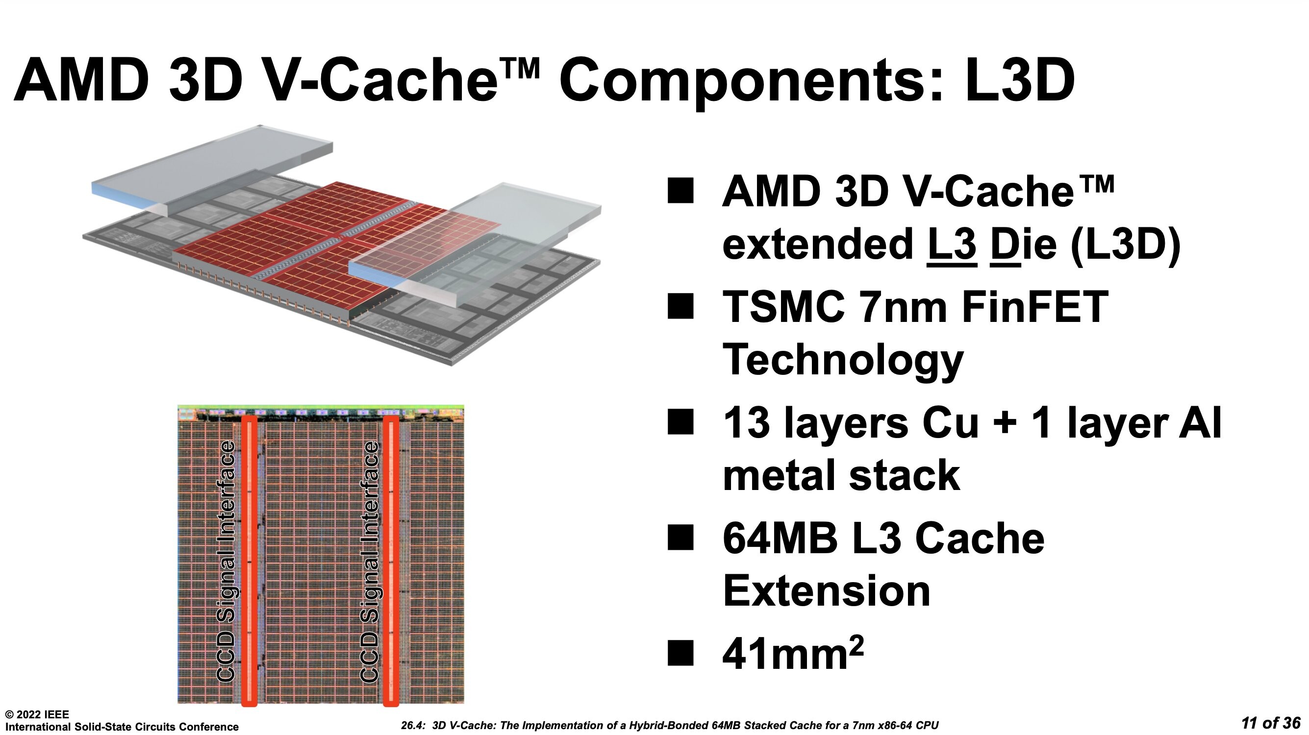
Update: A few more slides from AMD's presentation have made their way online, which gives away some additional details. First and foremost, the SRAM used for the 3D V-Cache is manufactured by TSMC on the N7 node. AMD is referring to it as an "extended L3 Die" in the slides as well as a 64 MB L3 cache extension. The 3D V-Cache SRAM measures 41mm2 and AMD has designed two additional structural supports of the CCD to help with thermal dissipation. To be able to fit everything into the same packaging as previous generation CPU's, AMD has had to thin the CCDs and L3 cache and the structural supports are also there to protect these thinned parts outside of the area covered by the 3D V-Cache.
If I can get ahold of a Ryzen 7 5800X3D when it releases I will test it.