This is recovery of the KPC Forums thread about GTX 680 Classified. Today in 2019 it gives a nice perspective what we had to do 7 years ago to achieve 2100 MHz GPU clock. Current Turing and Pascal GPUs we have achieve these clocks on aircooling out of the box!

STEP 0 - Overview
With GTX 680 CLASSIFIED there are two ways to get some nice OC. Easy way is to use digital controller, like
EVGA EVBOT to adjust settings on-fly during benching. Harder way is to use well-known trimpot, wires and other soldering mess to force card for higher performance.
Both ways violate your warranty and RMA rights for videocard, no matter what cooling was used, so as it is always with overclocking - do it on your own risk, provided AS IS. Killing hardware and sending back is no help for enthusiast community :P
For newbies, might be useful to check out
my reference GTX 680 overclocking/modification guide. It's still actual today and all described there apply to other GTX 680 designs as well. Component locations can differ but idea is exactly same.
As we all already know, Kepler family introduced Boost clock thing, which automatically increases graphics processor clock when there is headroom on thermals and power left unused. So for there three keystones important to understand for this technology function to enable overclocking.
First - is 3D loading level. If card just idle at desktop - clock and voltages will be kept low, minimizing power consumption. To get highest Boost clock you need to keep benchmark running while ensuring safe temperatures and voltages.
Second - temperature, if GPU running too hot - clock will throttle to safer levels, which will cap performance and will results lower benchmark score. With extreme overclocking right temperature is important as well, due fact that each GPU have different operation range. Some GPUs may refuse to boot/POST with -40°C, while
others can work like a charm even with -100°C. When card is running 3D app, like benchmark or game, it can go little colder temps. When we bench our cards, usually no problems to have -100 or -120°C during whole benchmark run. Learn your best temps for your card.
Third - power. All GTX 680 cards have special circuitry to measure +12V input power and constantly checking if that power level is below spec. If due to high temperature or high voltage your power reach that spec target - card throttle and reduce clock/workload. This is mostly main reason why aircooled/watercooled cards cannot reach over 1300-1400MHz, even when temperature stay cool. Also power limit make extreme overclocking useless due to big consumption increase with increased voltage. So bypassing this limit will be first task we do.
No matter if you use just EVBOT or do all-hardware modifications for voltage, you will need power limit bypass trick. So I will describe it first, before we dig deep.
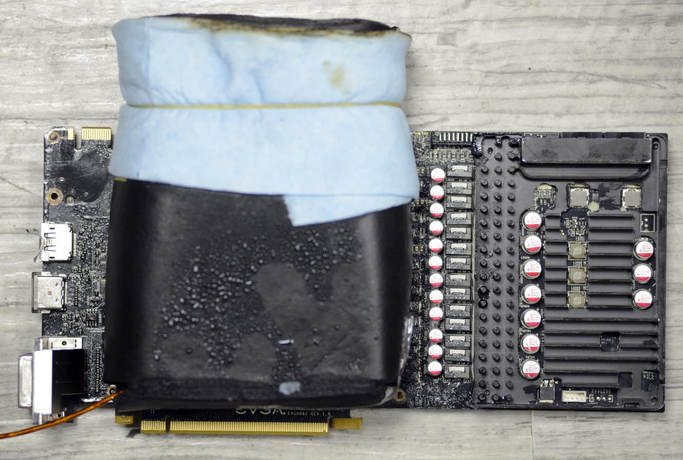
Power limit override To fool the power limitation set by NVIDIA for Kepler, we can reduce the resistance of current shunts. The reference card uses three 5 mohm resistors to measure input power, while CLASSIFIED use two 2 mohm resistor and 5 mohm for PCIe power.
If we short them or solder on an extra current shunt in parallel, we can decrease the power draw values reported to GPU. Also easier way might be to solder resistor to reduce current signal from sense resistor. There is a caveat though. On more modern GPUs like GTX780,980+ if shunt resistance is too low, card will detect this abnormal situation and throttle down to lowest clock possible. So more details how to overcome that shown here below. This is a must if you want to avoid being capped by power and TDP.
Let's check how power actually measured.
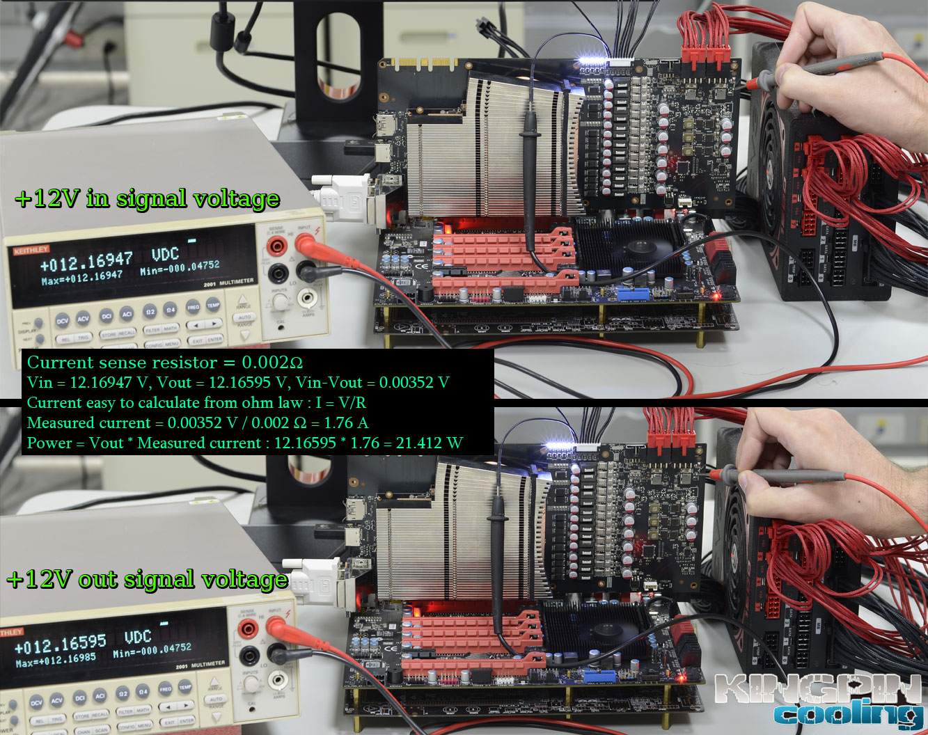
For that I use my DMM and measure both sides of sense resistor. As from ohm law when current flow thru some resistance there will be voltage drop, exactly proportional to resistance value. Our resistor is fixed at 0.002 ohm, and we can measure +12V input and output voltage on both ends, so calculating current is easy task even for 8-year old boy.
Here's math for one 8-pin power connector.
Current sense resistor = 0.002 ohm
Vin = 12.16947 V, Vout = 12.16595 V, Vin-Vout differential voltage = 0.00352 V
Current easy to calculate from ohm law : I = V/R
Measured current = 0.00352 V / 0.002 ohm = 1.76 A
Power 1 = Vout * Measured current : 12.16595 * 1.76 = 21.412 W
Second connector have same curcuitry with same 0.002 resistor, so approach is same
Current sense resistor = 0.002 ohm
Vin = 12.16892 V, Vout = 12.16615 V, Vin-Vout differential voltage = 0.00277 V
Current easy to calculate from ohm law : I = V/R
Measured current = 0.00352 V / 0.002 ohm = 1.385 A
Power 2 = Vout * Measured current : 12.16615 * 1.385 = 16.850 W
Total power consumed from +12V power
Power total = Power 1 + Power 2 = 21.412 + 16.850 = 38.262 W from +12V 8pin cables.
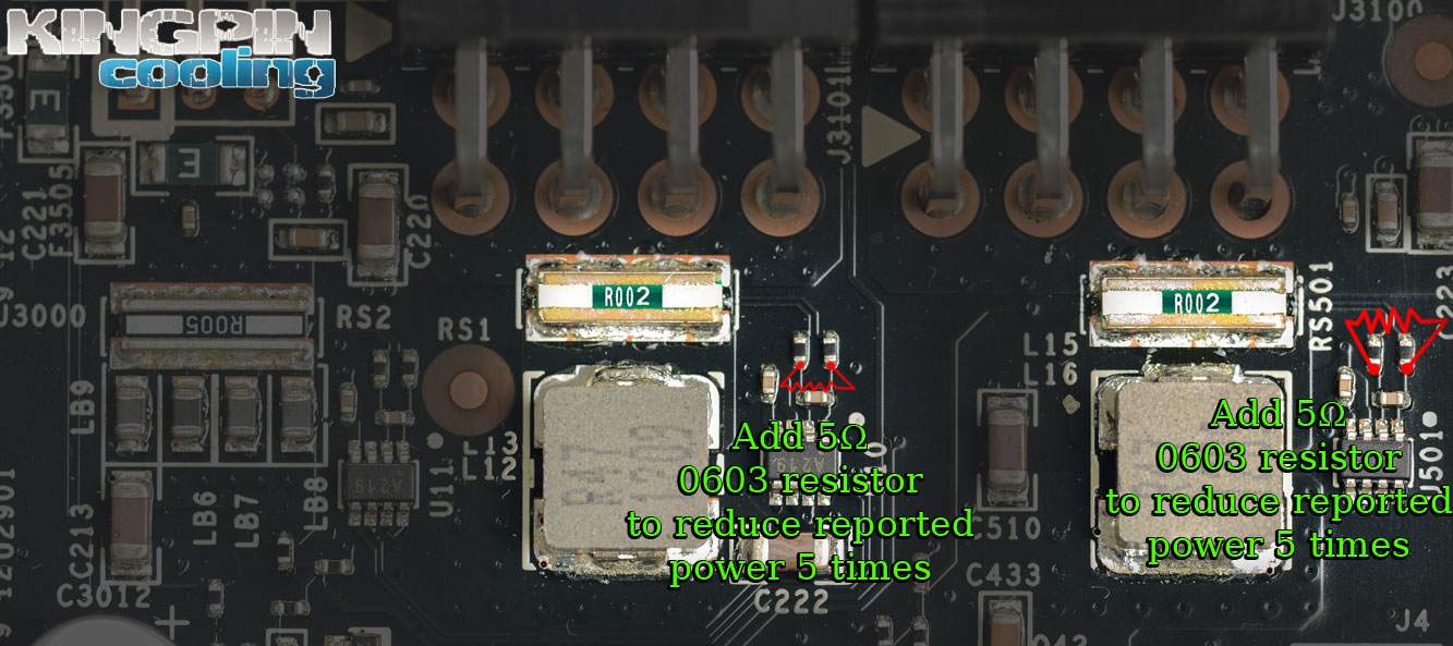
So Vin-Vout differential voltage is that signal which represent measured current. If we reduce it - we reduce read power. To do that we can shunt this voltage by extra resistor, for example 5 ohm - will reduce read ~10 times. Using same formula let's do math after this mod with 5 ohm resistor done:
Current sense resistor = 0.002 ohm with mod
Vin = 12.16808 V, Vout = 12.16774 V, Vin-Vout = 0.00034 V
Current easy to calculate from ohm law : I = V/R
Measured current = 0.00034 V / 0.002 ohm = 0.17 A
Power = Vout * Measured current : 12.16774 * 0.17 = 2.068 W
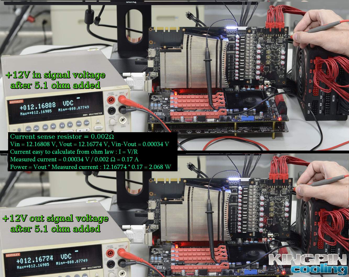
Finished mod with two 5.1 ohm resistor soldered:
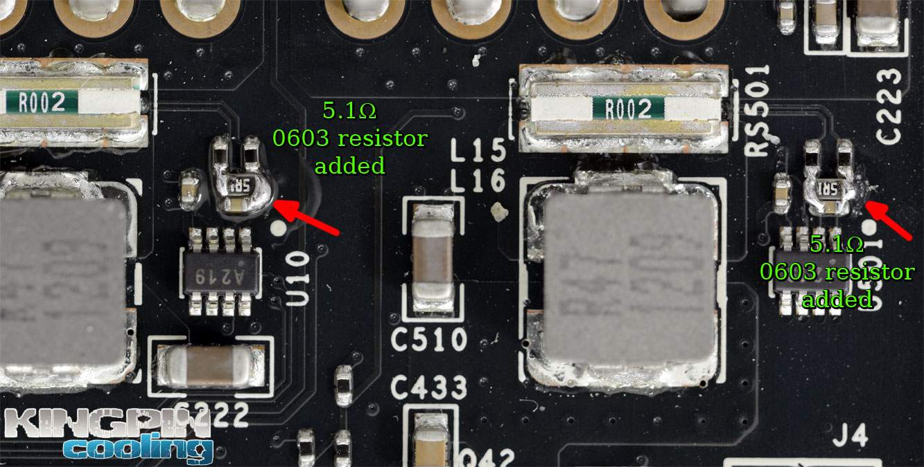
Now power levels detected by card will be much lower for each of power connectors. That mean if before power read was 200W, now it will be only 40W. According to actual power consumption, even under LN2 with 1.6Vgpu and 1700MHz card take around 500-600W max, so it should be enough to reach top speed even with extreme cooling. Smart guys might follow up with this modification and perform 0.005 modification as well, to reduce power from PCIe connector power.
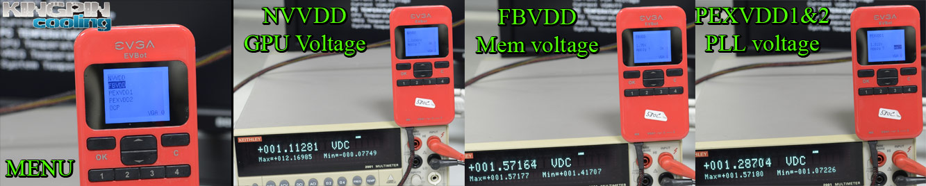
For voltage monitoring purposes EVGA GEFORCE GTX 680 CLASSIFIED have 10-pin 2 mm pitch connector near top PCB edge.
Pin definition:
Pin 1 - GPU voltage
Pin 2 - Ground
Pin 3 - MEM voltage
Pin 4 - Ground
Pin 5 - PLL voltage
Pin 6 - Ground
Pin 7 - Onboard +3.3V power voltage
Pin 8 - Ground
Pin 9 - Onboard +12V PCIe power voltage
Pin 10 - Ground
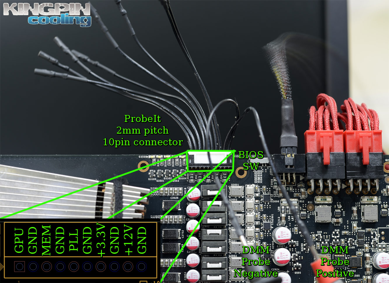
Also there BIOS switch nearby, which have three positions. Due to design requirements all BIOSes are same, but for extreme OC you should use BIOS SW toggled at location LN2.
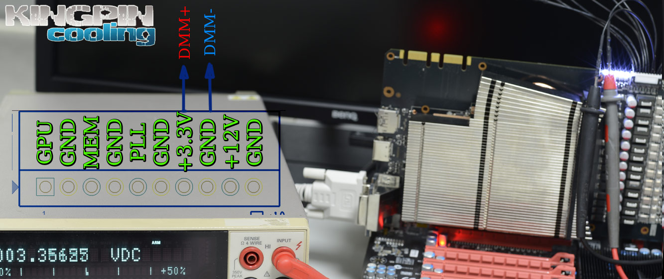
+3.3V monitoring:
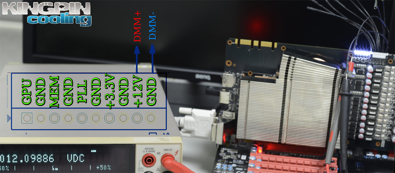
+12V monitoring:
Voltage modifications
WAY 1 - Easy EVBOT way Tool list:
2.54 mm dual-row header connector for newer GTX 680 Classifieds
Soldering iron with some solder and flux
Screwdrivers
Usual LN2 gear and TEK9 FAT 6.66
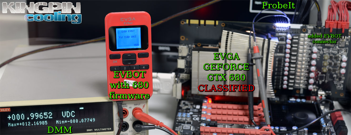
EVGA EVBOT
Digital multimeter to check voltages
STEP 1 Ensure you have
EVBOT with GTX 680 Classified firmware. If you have different one, you can use EVGA MB or CLASSIFIED 285/580/680 to reflash EVBOT. For that you can visit EVBOT page or get
GPU Flasher.
Due to safety reasons current GTX 680 CLASSIFIEDs do not have EVBOT connector populated. But pads still there on PCB, and with simple soldering job you can put standard 2.54 mm connector there. There is one pin removed on card for keying reason.

I would not be showing soldered connector, because I'm sure anyone can do that
 STEP 2
 EVBOT with 680 support have next controls:
* NVVDD - GPU voltage
* FBVDD - memory voltage
* PEXVDD1 - PLL first voltage
* PEXVDD2 - PLL second voltage
* OCP - use Extreme setting for LN2 sessions
For most LN2 benching 1.6-1.65V is more than enough to reach 1600-1700+ MHz with -70...-100°C temps on GPU code. Due to open die of GK104 good contact and tight mount is essential. With TEK9 FAT 6.66 pots we crank thumb nuts by hand as hard as possible without using tools. Sometimes card is bent like a banana after.
Optimal memory and PLL voltages depend on specific card, and you will need to try that yourself to see if it gain help.
STEP 3 Enhancements
WAY 2 - For those poor souls who always cry about extra cost added by EVBOT Soldering iron with some solder and flux
Screwdrivers
Usual LN2 gear and TEK9 FAT 6.66
Multiturn VRs with 1kohm resistance
Thin AWG30 wire for connections
Digital multimeter to check voltages
STEP 1 Locate some areas.
STEP 2 Prep some parts
10K VR for memory mod
50K VR for PEXVDD1 mod
50K VR for PEXVDD2 mod
two 5.1K 0603 SMD resistors for power limiter mod
STEP 3 GPU voltage modification
I like VID modifications, because they always work and don't trip protection functions when voltage being increased. So it's exactly same idea as on reference GTX 680 modification guide so I will only show difference:
To be able to toggle VID i used pullup resistors 4.7kohm to +3.3V, so when switch position open - i get logical "1" on VID signal, if position shorted - logical "0". Then task simplifies to just finding correct code and setting proper levels for switch.
Here how it was on NVIDIA reference GTX 680:
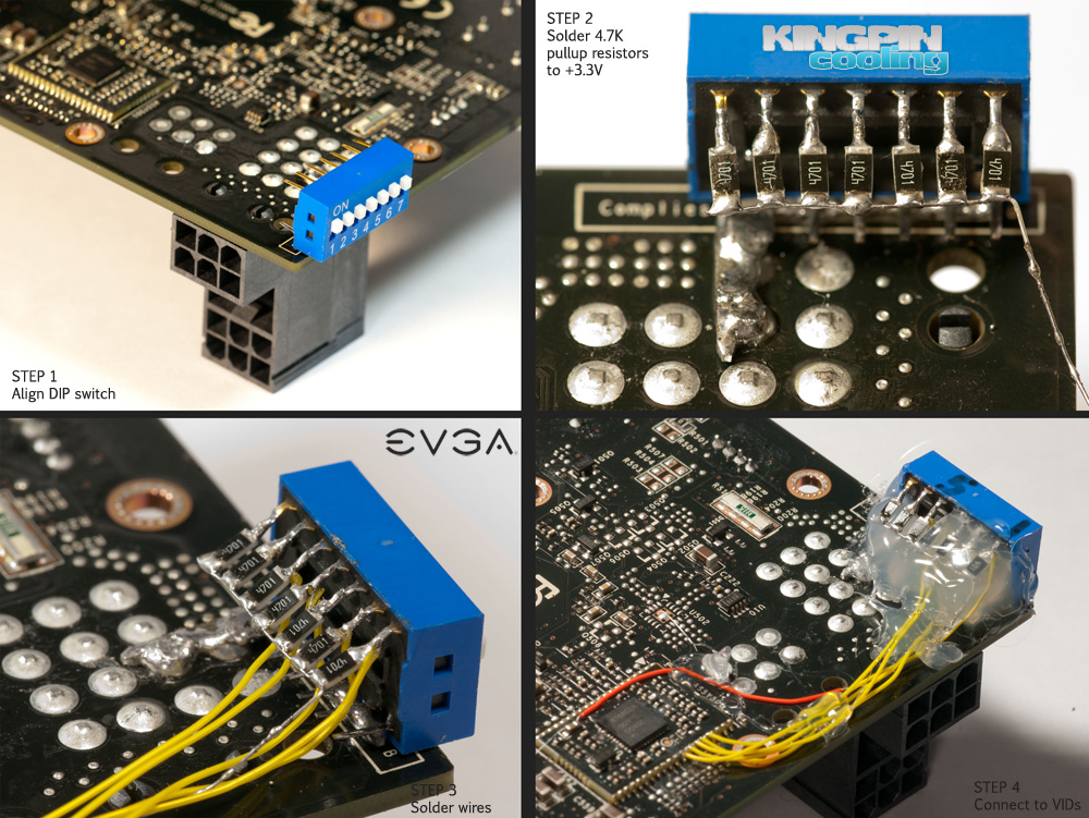
Here how it is on EVGA GTX 680 CLASSIFIED:
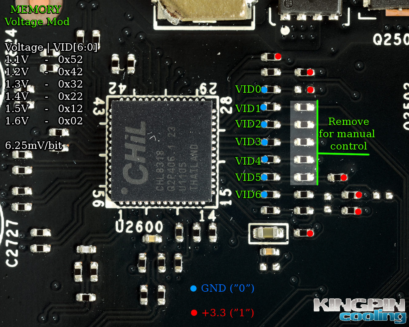
Red dots - +3.3V points, blue - GND points. By populating or removing proper resistors you can easy change VID value. To get always fixed voltage no matter what - remove 5 resistors in lightgray box.
STEP 4 Memory voltage modification
Power for memory is generated by 3-phase switching unit. It's located near bottom left corner of PCB on front side. Memory voltage is controlled by 2D/3D mode as well, so in 2D/idle you will see ~1.4V, while under load it reaches 1.6V. By doing feedback modification we increase both voltages.

Stock resistance on marked pin is 607 ohm. This modification use 10 Kohm resistance. 6.8K can work too, if you want finer adjustment steps. Don't forget to set VR's to max resistance between used pins first.
STEP 5 PLL voltages modification
PLL Power is used for internal units in GPU and for PCI-Express interface operation. Increasing this voltages can be useful for extreme overclocking with subzero cooling. You may check behavior of your specific card when adjust this voltages.
PLL Voltages generated by simple LDO IC, one per each rail. Knowing this it's easy to find feedback pin and change resistance with VR to increase output voltage for PEXVDD1 and PEXVDD2 parts.
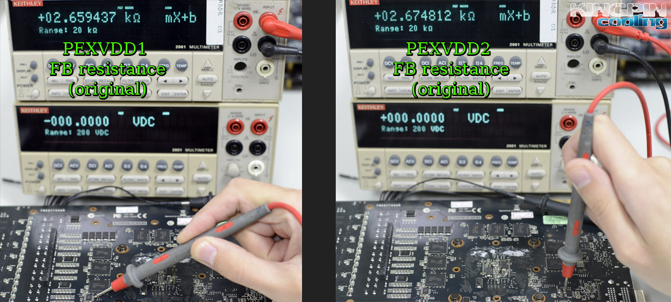
Here's original resistance on feedback pins (Pin 7) related to GND (Pin 8).
PEXVDD1 - original 2.659 Kohm
PEXVDD2 - original 2.674 Kohm
To increase voltage we need to reduce resistance. As usual follow rule 1:10 for VR resistance value choice. This mean we will need 47K or 50K VR. Best to use multiturn VRs, I use 3296W type.
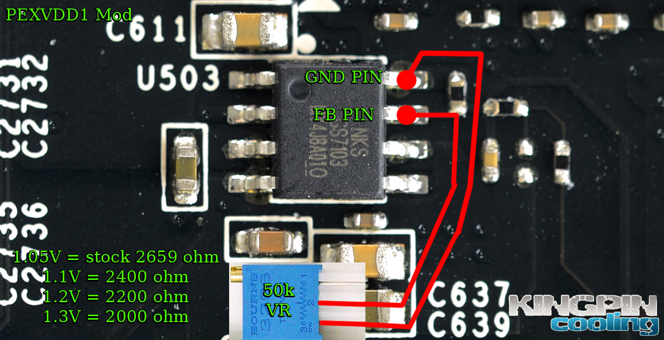
Part one. IC is SO8 package so it's not hard to solder to it's pins.
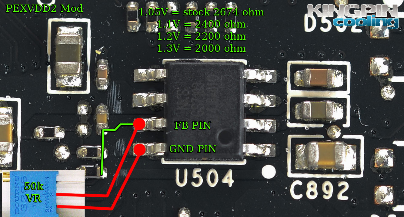
Part two, PEXVDD2 - same approach.
Both of these areas located on back side of card, near PCIe edge connector.
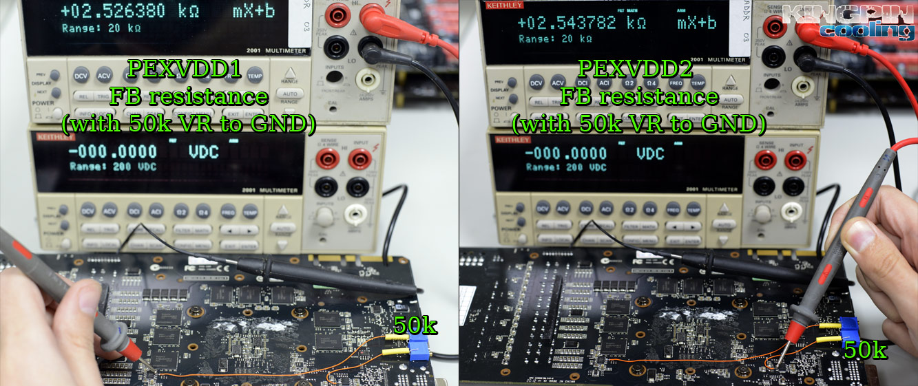
After correct modification resistance on both FB pins should be little lower. If you have big difference - double check your work again. Don't forget to set VR's to max resistance between used pins first.
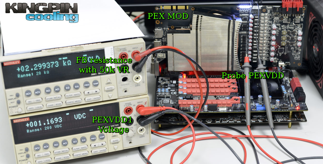
Check again, and then power on card with mod. Stock voltage with 2.3Kohm on FB is near 1.17V now.
STEP 6 Now card ready to crack:
---
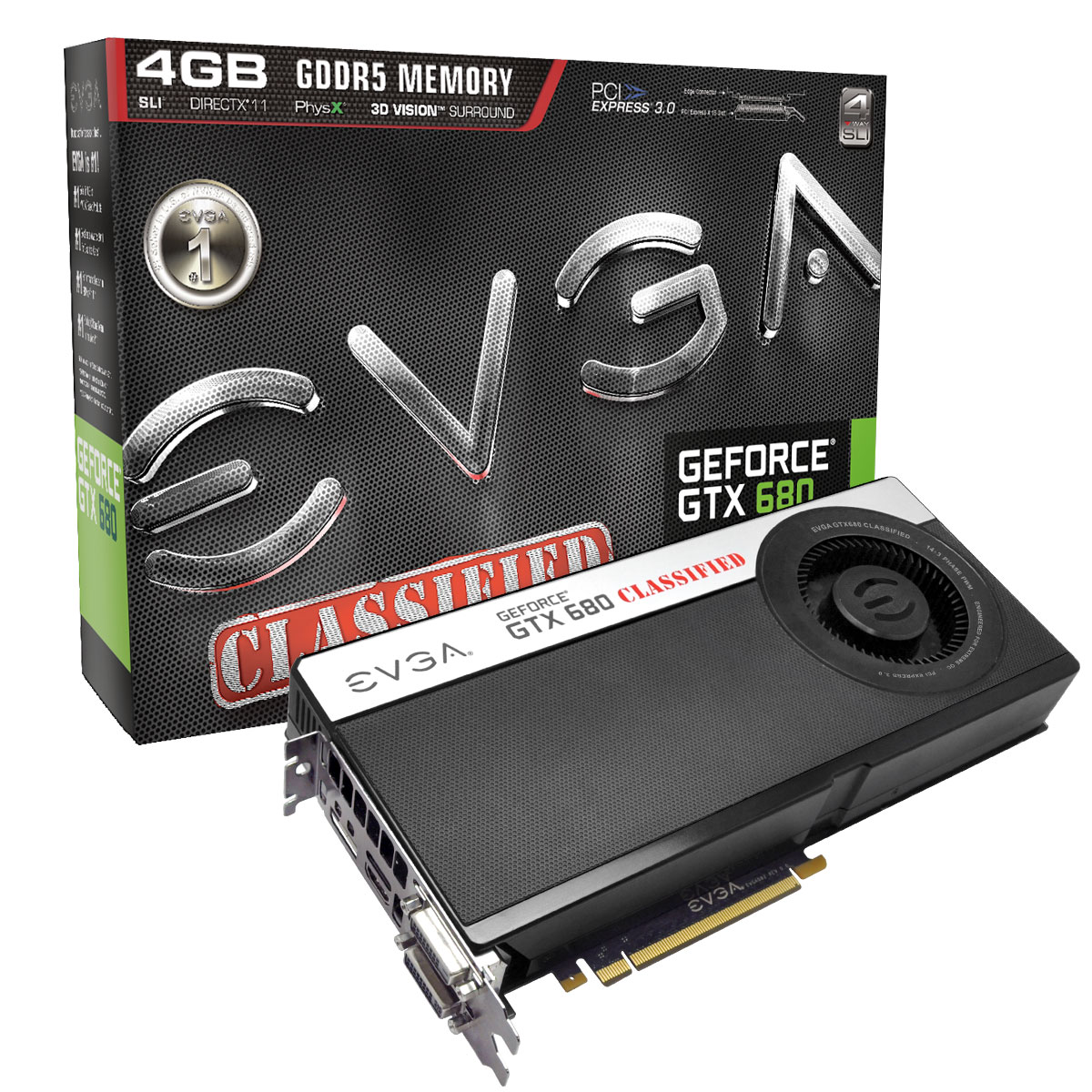
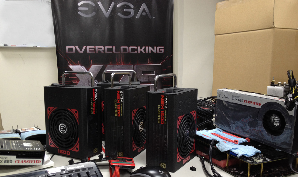
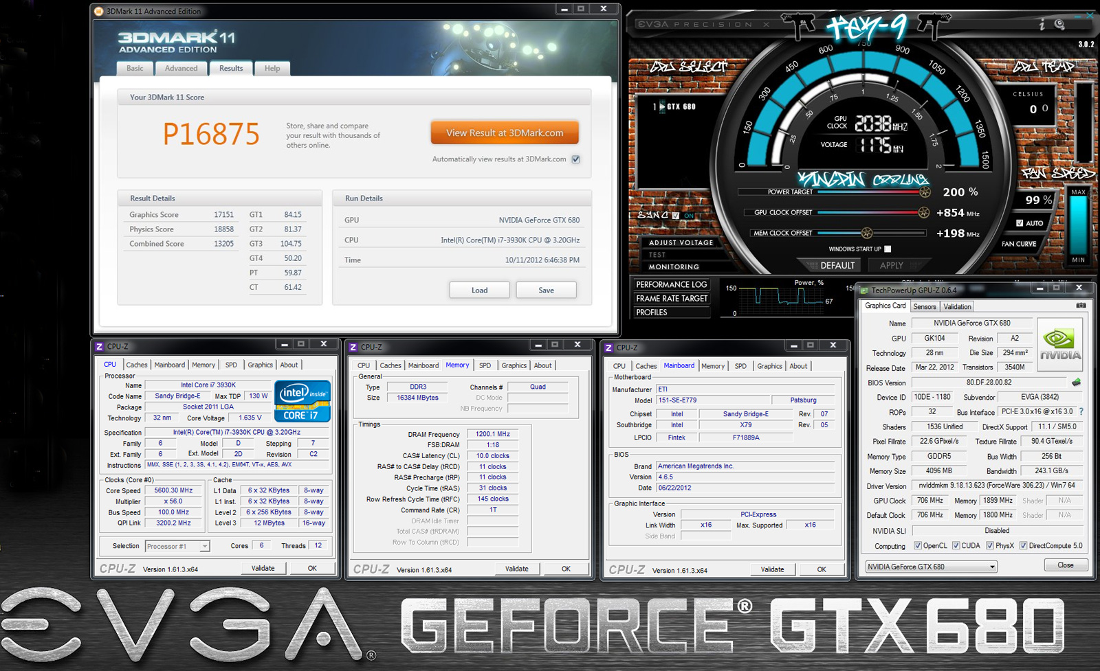
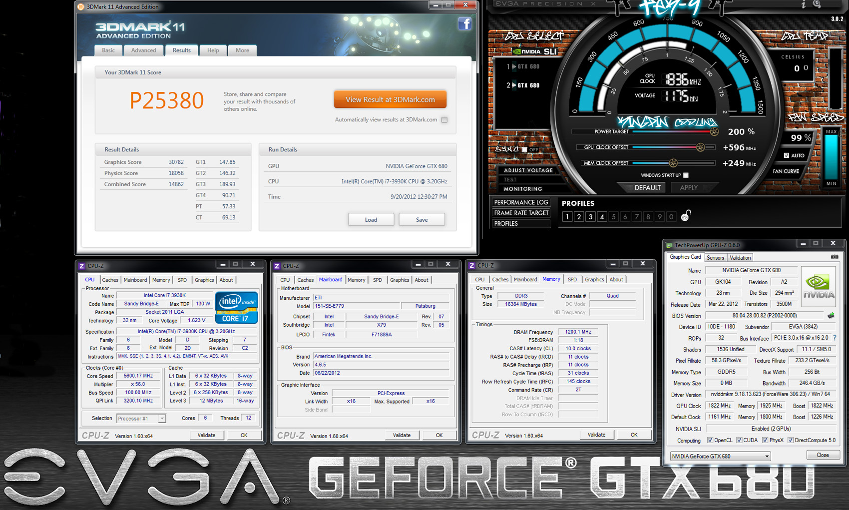
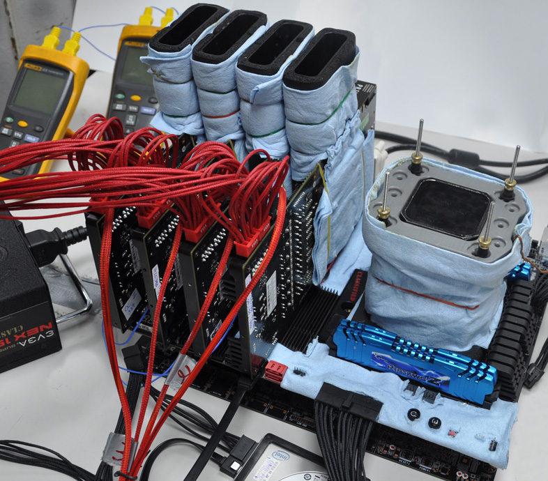
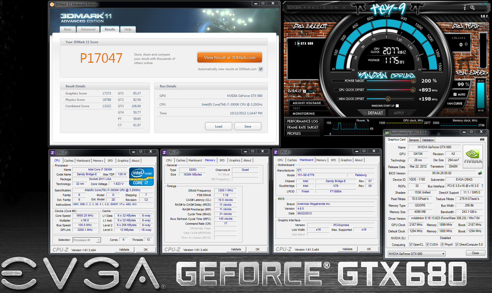
Time to overclock EVGA GTX 680 CLASSIFIED again, benching hard for 2100mhz and 17K + single card atm, that's the new target. Feel like I'm starting to close in on it now. Classy 680 also takes SLI and QUAD SLI 3DMARK 11 Futuremark records. OCTV spent a week with me in my lab filming tons of benching for EVGA's new overclocking video due out later this month. They captured some really great benching footage including single, SLI, and quad 3d11 world records. More on that as we get closer to launch of the video and there will also be a REALLY nice giveaway by EVGA/KPC to celebrate the launch of the video. Official announcement soon
. TiN will be posting up some CLASSY HW modifications guides today to help get u guys up to speed with some workarounds and there will also be some nice updates to precision that many of you will like. A ton of work and time was put into getting speeds like these and its been almost non stop over here. Hope u dig it...from the start its been our goal to design and manuf the baddest NVIDIA 680 card on the planet without limits. This is still something we are working towards and hopeful of

Hardware:
EVGA CLASSIFIED GTX 680 in single, sli, and quad sli.
EVGA CLASSIFIED X79 + 3930K
GSKILL RIPJAWS-Z 16GB
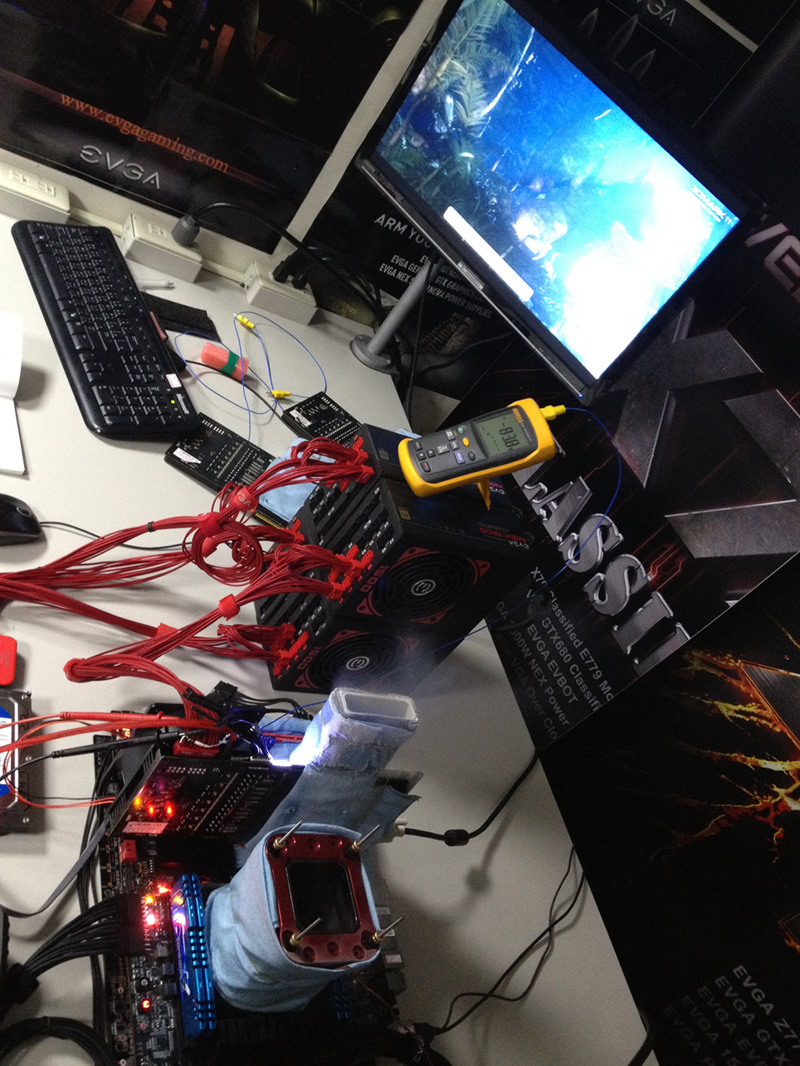
EVGA NEX 1500W PSU (x4 in quad
)
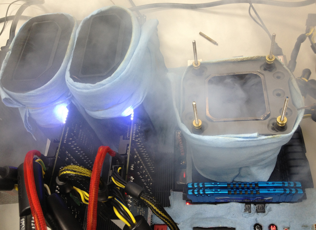
KPC DRAGON F1 DARK cpu pot
TEK-9 FAT gpu pot
TEK-9 SLIMS (quad sli)
Fastest GPU on the planet!
Nex 1500W is nice to bench multi psu's with using dummy mode switch on back and modular cables
Almost 17k single gpu 3D11 now, card is screaming:
P25380 @1840mhz SLI on Dual TEK-9 FAT gpu units
Card pretesting for quad on slim units..
X17384 QUAD SLI
3DMARK HOF X 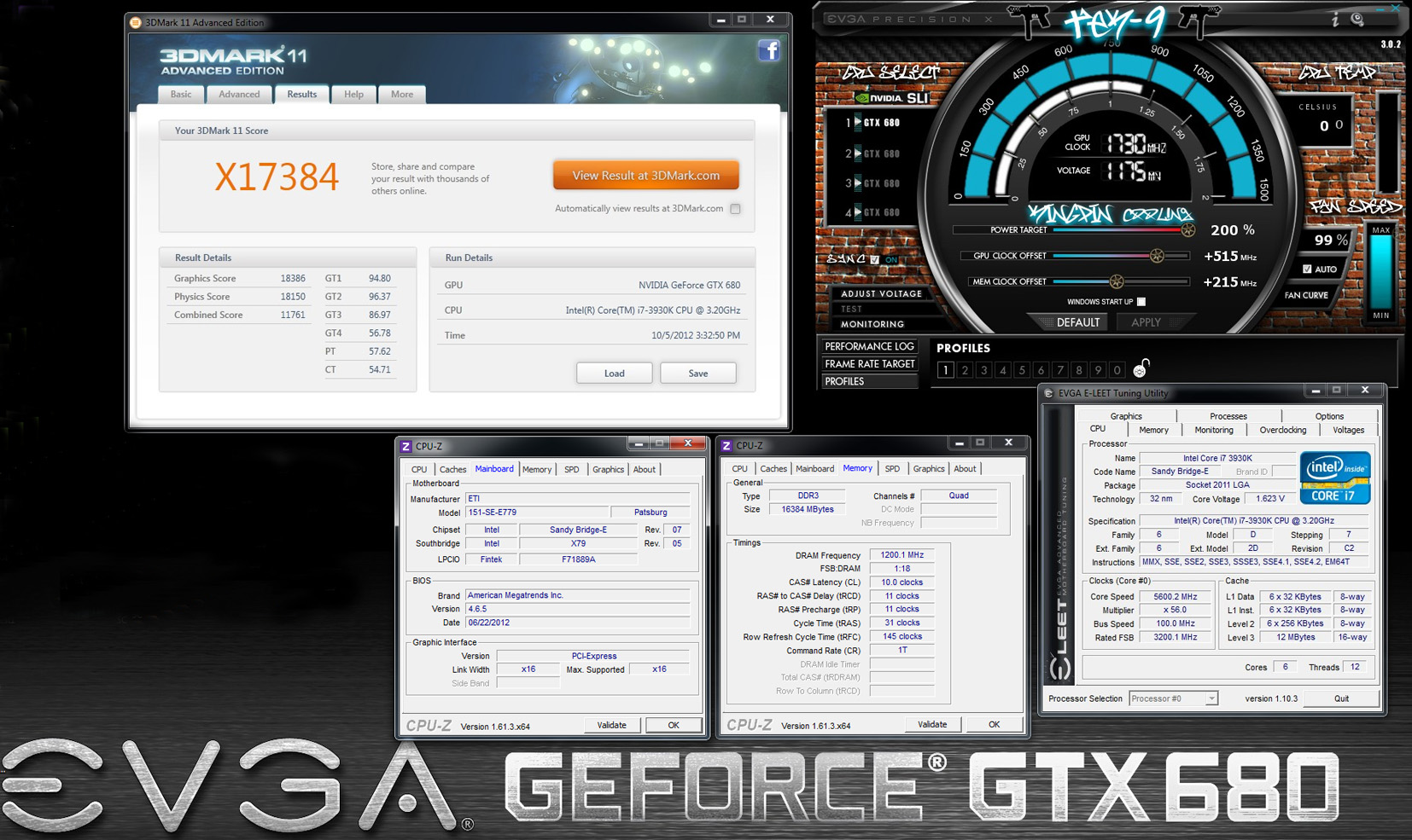
QUAD SLI rig
CLASSY 680 does 17k single card 11..only took 2080mhz

post edited by TiN_EE - 2019/02/11 03:02:59